Материал: 9763
DISCRETE SEMICONDUCTORS
M3D176
BAX18
General purpose diode
Product specification |
1996 Apr 17 |
Supersedes data of April 1992
File under Discrete Semiconductors, SC01
Philips Semiconductors |
Product specification |
|
|
|
|
General purpose diode |
BAX18 |
|
|
|
|
FEATURES
∙Hermetically sealed leaded glass SOD27 (DO-35) package
∙Switching speed: max. 50 ns
∙General application
∙Continuous reverse voltage: max. 75 V
∙Repetitive peak reverse voltage: max. 75 V
∙Repetitive peak forward current: max. 2 A
∙Forward voltage: max. 1 V.
APPLICATIONS
∙ Rectifier applications.
DESCRIPTION
The BAX18 is a general purpose diode fabricated in planar technology, and encapsulated in the hermetically sealed leaded glass SOD27 (DO-35) package.
k |
a |
handbook, halfpage |
|
MAM246
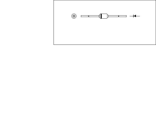
The diode is type branded.
Fig.1 Simplified outline (SOD27; DO-35) and symbol.
LIMITING VALUES
In accordance with the Absolute Maximum Rating System (IEC 134).
SYMBOL |
PARAMETER |
CONDITIONS |
MIN. |
MAX. |
UNIT |
|
|
|
|
|
|
VRRM |
repetitive peak reverse voltage |
|
− |
75 |
V |
VR |
continuous reverse voltage |
|
− |
75 |
V |
IF |
continuous forward current |
see Fig.2; note 1 |
− |
500 |
mA |
IFRM |
repetitive peak forward current |
|
− |
2000 |
mA |
IFSM |
non-repetitive peak forward current |
square wave; Tj = 25 °C prior to |
|
|
|
|
|
surge; see Fig.4 |
|
|
|
|
|
t = 1 μs |
− |
55 |
A |
|
|
t = 100 μs |
− |
15 |
A |
|
|
t = 10 ms |
− |
9 |
A |
|
|
|
|
|
|
Ptot |
total power dissipation |
Tamb = 25 °C; note 1 |
− |
450 |
mW |
Tstg |
storage temperature |
|
−65 |
+200 |
°C |
Tj |
junction temperature |
|
− |
200 |
°C |
Note
1. Device mounted on an FR4 printed circuit-board; lead length 10 mm.
1996 Apr 17 |
2 |

Philips Semiconductors |
|
|
Product specification |
|||
|
|
|
|
|
|
|
General purpose diode |
|
|
|
BAX18 |
||
|
|
|
|
|
|
|
ELECTRICAL CHARACTERISTICS |
|
|
|
|
|
|
Tj = 25 °C; unless otherwise specified. |
|
|
|
|
|
|
|
|
|
|
|
|
|
SYMBOL |
PARAMETER |
CONDITIONS |
MIN. |
MAX. |
|
UNIT |
|
|
|
|
|
|
|
VF |
forward voltage |
see Fig.3 |
|
|
|
|
|
|
IF = 300 mA |
− |
1.0 |
|
V |
|
|
IF = 2 A; Tj = 150 °C |
− |
1.5 |
|
V |
IR |
reverse current |
see Fig.5 |
|
|
|
|
|
|
VR = 75 V |
− |
5 |
|
μA |
|
|
VR = 75 V; Tj = 150 °C |
− |
100 |
|
μA |
Cd |
diode capacitance |
f = 1 MHz; VR = 0; see Fig.6 |
− |
35 |
|
pF |
trr |
reverse recovery time |
when switched from IF = 30 mA to |
− |
50 |
|
ns |
|
|
IR = 30 mA; RL = 100 Ω; |
|
|
|
|
|
|
measured at IR = 3 mA; see Fig.7 |
|
|
|
|
THERMAL CHARACTERISTICS
SYMBOL |
PARAMETER |
CONDITIONS |
VALUE |
UNIT |
|
|
|
|
|
Rth j-tp |
thermal resistance from junction to tie-point |
lead length 10 mm |
240 |
K/W |
Rth j-a |
thermal resistance from junction to ambient |
lead length 10 mm; note 1 |
375 |
K/W |
Note
1. Device mounted on a printed circuit-board without metallization pad.
1996 Apr 17 |
3 |
Philips Semiconductors |
Product specification |
|
|
General purpose diode |
BAX18 |
|
|
GRAPHICAL DATA
500 |
|
|
|
|
|
MBG455 |
|
|
|
|
|
|
|
handbook, halfpage |
|
|
|
|
|
|
IF |
|
|
|
|
|
|
(mA) |
|
|
|
|
|
|
400 |
|
|
|
|
|
|
300 |
|
|
|
|
|
|
200 |
|
|
|
|
|
|
100 |
|
|
|
|
|
|
0 |
|
|
|
o |
|
|
0 |
100 |
Tamb |
( |
C) |
200 |
|
|
|
|
|
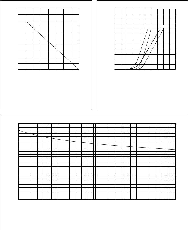
Device mounted on an FR4 printed-circuit board; lead length 10 mm.
Fig.2 Maximum permissible continuous forward current as a function of ambient temperature.
MBG467
3 handbook, halfpage
IF
(A)
(1) |
(2) |
(3) |
(4) |
2
1
0
0 |
1 |
VF |
(V) |
2 |
|
|
|
(1)Tj = 175 °C; typical values.
(2)Tj = 25 °C; typical values.
(3)Tj = 150 °C; maximum values.
(4)Tj = 25 °C; maximum values.
Fig.3 Forward current as a function of forward voltage.
MBG702
102 handbook, full pagewidth
IFSM
(A)
10
1
10−1
1 |
10 |
102 |
103 |
tp (μs) |
104 |
|
|
|
|
|
Based on square wave currents.
Tj = 25 °C prior to surge.
Fig.4 Maximum permissible non-repetitive peak forward current as a function of pulse duration.
1996 Apr 17 |
4 |
Philips Semiconductors |
Product specification |
|
|
General purpose diode |
BAX18 |
|
|
104 |
MBG697 |
|
|
|
handbook, full pagewidth
IR
(μA)
103
102
10
1
10−1
10−2
0 |
100 |
Tj (oC) |
200 |
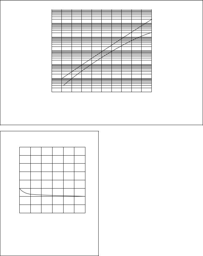
VR = 75 V.
Solid line; maximum values. Dotted line; typical values.
Fig.5 Reverse current as a function of junction temperature.
MGD003
40 handbook, halfpage
Cd (pF)
30
20
10
0
0 |
10 |
20 |
30 |
|
|
VR |
(V) |
f = 1 MHz; Tj = 25 °C.
Fig.6 Diode capacitance as a function of reverse voltage; typical values.
1996 Apr 17 |
5 |