Материал: MAC15S
MOTOROLA
SEMICONDUCTOR TECHNICAL DATA
Order this document by MAC15S/D
Advance Information
TRIACS
Silicon Bidirectional Thyristors
Designed for industrial and consumer applications for full wave control of ac loads such as appliance controls, heater controls, motor controls, and other power switching applications.
•Sensitive Gate allows Triggering by Microcontrollers and other Logic Circuits
•High Immunity to dv/dt Ð 25 V/ ms minimum at 110_C
•High Commutating di/dt Ð 8.0 A/ms minimum at 110 _C
•Minimum and Maximum Values of IGT, VGT and IH specified for ease of design
•On-State Current Rating of 15 Amperes RMS at 70_C
•High Surge Current Capability Ð 120 Amperes
•Blocking Voltage to 800 Volts
•Rugged, Economical TO220AB Package
MAXIMUM RATINGS (TJ = 25°C unless otherwise noted)
MAC15S SERIES
TRIACS
15 AMPERES RMS
400 THRU 800
VOLTS
MT2
MT1 
MT2 

G
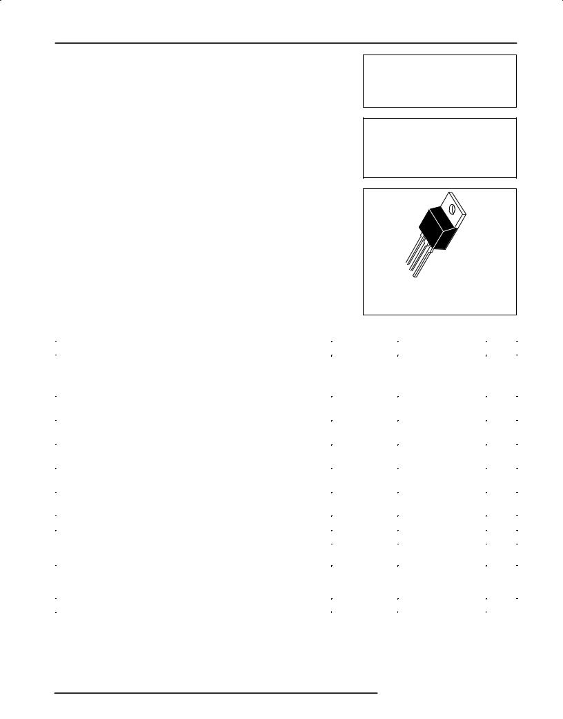
CASE 221A±06 (TO-220AB)
STYLE 4
Parameter |
|
Symbol |
Value |
Unit |
|
|
|
|
|
Peak Repetitive Off-State Voltage (1) |
|
VDRM |
|
Volts |
(TJ = ±40 to 110°C, Sine Wave, 50 to 60Hz, Gate Open) |
MAC15SD |
|
400 |
|
|
MAC15SM |
|
600 |
|
|
MAC15SN |
|
800 |
|
|
|
|
|
|
On-State RMS Current |
|
IT(RMS) |
15 |
A |
(Full Cycle Sine Wave, 60Hz, TJ = 70°C) |
|
|
|
|
Peak Non-repetitive Surge Current |
|
ITSM |
120 |
A |
(One Half Cycle, 60 Hz, TJ = 110°C) |
|
|
|
|
Circuit Fusing Consideration |
|
I2t |
60 |
A2sec |
(t = 8.3 ms) |
|
|
|
|
|
|
|
|
|
Peak Gate Power |
|
PGM |
20 |
Watts |
(Pulse Width ≤ 1.0 ms, TC = 70°C) |
|
|
|
|
Average Gate Power |
|
PG(AV) |
0.5 |
Watts |
(t = 8.3 ms, TC = 70°C) |
|
|
|
|
Operating Junction Temperature Range |
|
TJ |
± 40 to +110 |
°C |
Storage Temperature Range |
|
Tstg |
± 40 to +150 |
°C |
THERMAL CHARACTERISTICS
Thermal Resistance |
|
|
°C/W |
Ð Junction to Case |
RqJC |
2.0 |
|
Ð Junction to Ambient |
RqJA |
62.5 |
|
Maximum Lead Temperature for Soldering Purposes 1/8″ from Case for 5 Seconds |
TL |
260 |
°C |
(1) VDRMforalltypescanbeappliedonacontinuousbasis.Blockingvoltagesshallnotbetestedwithaconstantcurrentsourcesuchthatthevoltage
ratings of the devices are exceeded.
REV 0
Motorola, Inc. 1995
MAC15S |
SERIES |
|
|
|
|
||
ELECTRICAL CHARACTERISTICS (TJ = 25°C unless otherwise noted) |
|
|
|
|
|||
|
|
|
|
|
|
|
|
Characteristic |
|
|
Symbol |
Min |
Typ |
Max |
Unit |
|
|
|
|
|
|
|
|
OFF CHARACTERISTICS |
|
|
|
|
|
|
|
|
|
|
|
|
|
|
|
Peak Repetitive Blocking Current |
TJ = 25°C |
IDRM |
Ð |
Ð |
0.01 |
mA |
|
(VD = Rated VDRM, Gate Open) |
|
|
|||||
|
TJ = 110°C |
|
Ð |
Ð |
2.0 |
|
|
ON CHARACTERISTICS |
|
|
|
|
|
|
|
|
|
|
|
|
|
|
|
Peak On-State Voltage* (ITM = 21A) |
|
|
VTM |
Ð |
Ð |
1.8 |
Volts |
Continuous Gate Trigger Current (VD = 12 V, RL = 100Ω) |
|
|
IGT |
.8 |
2.0 |
5.0 |
mA |
MT2(+), G(+) |
|
|
|
|
|||
MT2(+), G(±) |
|
|
|
.8 |
3.0 |
5.0 |
|
MT2(±), G(±) |
|
|
|
.8 |
3.0 |
5.0 |
|
|
|
|
|
|
|
|
|
Hold Current (VD = 12 V, Gate Open, Initiating Current = 150mA) |
|
IH |
1.0 |
3.0 |
10 |
mA |
|
Latching Current (VD = 24V, IG = 5mA) |
|
|
IL |
2.0 |
5.0 |
15 |
mA |
MT2(+), G(+) |
|
|
|
|
|||
MT2(+), G(±) |
|
|
|
2.0 |
10 |
20 |
|
MT2(±), G(±) |
|
|
|
2.0 |
5.0 |
15 |
|
|
|
|
|
|
|
|
|
Gate Trigger Voltage (Continuous dc) (VD = 12 V, RL = 100Ω) |
|
|
VGT |
0.45 |
0.62 |
1.5 |
Volts |
MT2(+), G(+) |
|
|
|
|
|||
MT2(+), G(±) |
|
|
|
0.45 |
0.60 |
1.5 |
|
MT2(±), G(±) |
|
|
|
0.45 |
0.65 |
1.5 |
|
|
|
|
|
|
|
|
|
DYNAMIC CHARACTERISTICS |
|
|
|
|
|
|
|
|
|
|
|
|
|
|
|
Critical Rate of Rise of Off±State Voltage |
|
|
(dv/dt)c |
8.0 |
10 |
Ð |
A/ms |
(VD = 400V, ITM = 3.5A, Commutating dv/dt = 10Vm/sec, |
|
|
|
|
|
|
|
Gate Open, TJ = 110_C, f= 500Hz, Snubber: CS = 0.01 mF, RS =15W, |
|
|
|
|
|
|
|
see figure 15. ) |
|
|
|
|
|
|
|
|
|
|
|
|
|
|
|
Critical Rate of Rise of Off-State Voltage |
|
|
dv/dt |
25 |
75 |
Ð |
V/ms |
(VD = Rate VDRM, Exponential Waveform, RGK = 510W, TJ = 110_C) |
|
|
|
|
|
|
|
* Indicates Pulse Test: Pulse Width ≤ 2.0 ms, Duty Cycle ≤ 2%. |
|
|
|
|
|
|
|
,MAXIMUM ALLOWABLE CASE TEMPERATURE (C)° |
110 |
|
|
|
|
|
|
|
|
|
, MAXIMUM AVERAGE POWER DISSIPATION(WATTS) |
25 |
100 |
|
|
|
|
|
|
|
|
|
20 |
||
|
|
|
|
|
|
|
a = 30 and 60° |
|
||||
90 |
|
|
|
|
|
|
|
|
|
15 |
||
|
|
|
|
α |
|
|
|
|
|
|
||
80 |
|
|
α |
|
|
|
|
|
|
10 |
||
|
|
a = CONDUCTION ANGLE |
|
120° |
|
|
|
|
||||
|
|
|
|
|
|
|
|
|||||
70 |
|
|
|
|
|
|
|
|
180° |
5 |
||
|
|
|
|
|
|
|
|
|
|
|||
60 |
|
|
|
|
|
|
|
|
DC |
0 |
||
0 |
2 |
4 |
6 |
8 |
10 |
12 |
14 |
16 |
||||
C |
|
|
|
IT(RMS), RMS ON±STATE CURRENT (AMPS) |
|
|
(AV) |
|
||||
T |
|
|
|
|
|
P |
|
|||||
|
|
|
α |
|
|
|
DC |
|
|
|
|
|
|
180° |
|
|
|
|
|
α |
|
|
|
|
|
|
|
|
|
|
|
120° |
|
|
|
|
|
|
|
|
|
|
|
|
|
a = CONDUCTION ANGLE |
|
90° |
|
|
|
||
|
|
60° |
|
|
|
|||
|
|
|
|
|
|
|
|
|
|
|
|
|
|
|
|
a = 30° |
|
0 |
2 |
4 |
6 |
8 |
10 |
12 |
14 |
16 |
|
|
IT(RMS), RMS ON±STATE CURRENT (AMPS) |
|
|||||
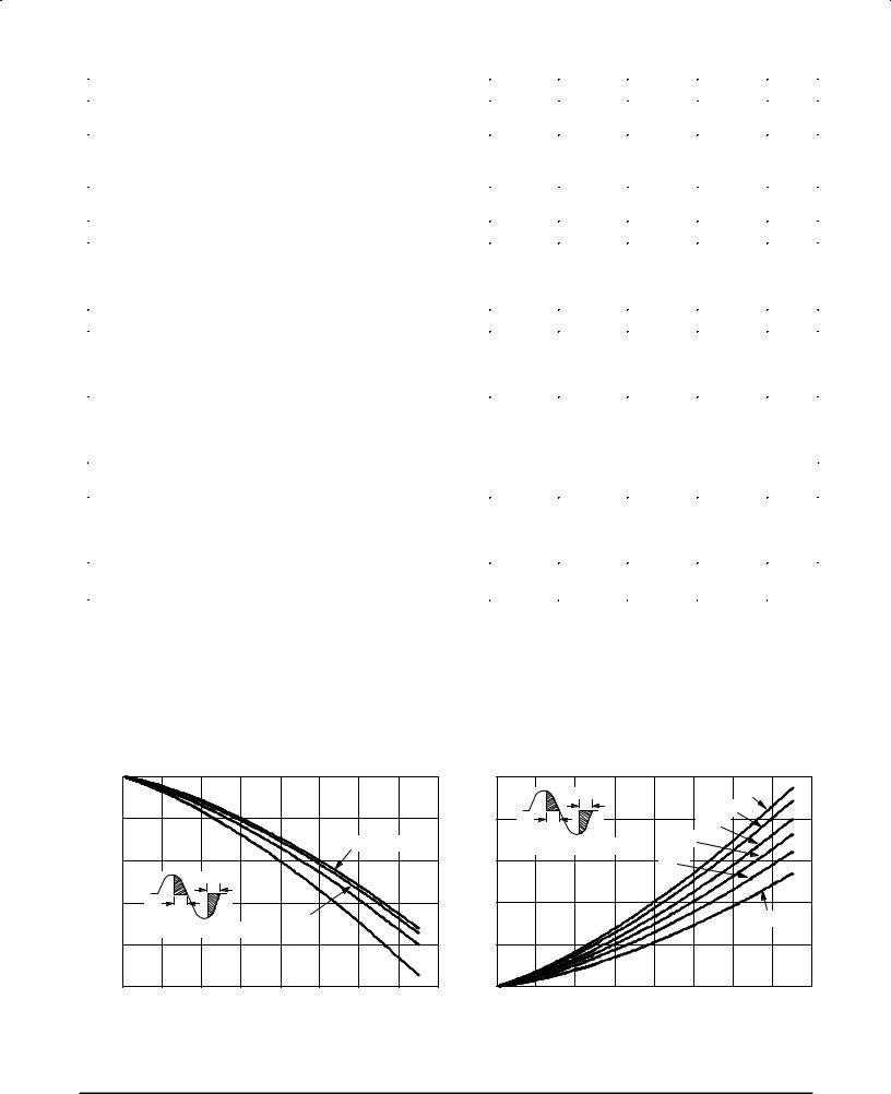
Figure 1.0 RMS Current Derating |
Figure 2.0 Maximum On±State Power Dissipation |
Data Sheets |
2 |
Motorola Thyristor Device Data |
(AMPS)CURRENTSTATE-ONINSTANTANOUS |
|
|
|
|
|
|
|
MAC15S |
SERIES |
|
|
|
|
|
||
100 |
Typical @ TJ = 25 °C |
|
|
|
|
|
|
(NORMALIZED)RESISTANCETHERMAL |
1 |
|
|
|
|
|
||
|
|
|
|
|
|
|
|
|
|
|
|
|
||||
|
|
|
|
|
|
|
|
|
|
|
|
|
|
|
||
|
10 |
|
|
Maximum @ |
|
|
|
|
|
|
|
ZqJC(t) = RqJC(t) r(t) |
|
|
||
|
|
|
|
TJ = 25 °C |
|
|
|
|
|
|
|
|
|
|
|
|
|
|
|
|
|
|
|
|
|
|
|
0.1 |
|
|
|
|
|
|
1 |
|
Maximum @ |
|
|
|
|
|
|
|
|
|
|
|
|
|
|
|
|
|
|
|
|
|
|
|
|
|
|
|
|
||
|
|
|
TJ = 110°C |
|
|
|
|
|
,TRANSIENT |
|
|
|
|
|
|
|
I |
0.5 |
1 |
1.5 |
2 |
2.5 |
3 |
3.5 |
4 |
4.5 |
0.1 |
1 |
10 |
100 |
1000 |
1@104 |
|
, |
0.1 |
|
|
|
|
|
|
|
|
|
0.01 |
|
|
|
|
|
T |
|
|
|
|
|
|
|
|
|
|
|
|
|
|
|
|
|
|
VT, INSTANTANEOUS ON±STATE VOLTAGE (VOLTS) |
|
(t) |
|
|
t, TIME (ms) |
|
|
|
||||||
|
|
|
R |
|
|
|
|
|
||||||||
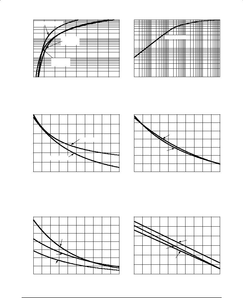
Figure 3.0 On±State Characteristics |
Figure 4.0 Transient Thermal Response |
|
7 |
|
|
|
|
|
|
|
|
|
|
9 |
|
|
|
|
|
|
|
|
|
|
HOLDING CURRENT (mA) |
6 |
|
|
|
|
|
|
|
|
|
LATCHING CURRENT (mA) |
8 |
|
|
|
|
|
|
|
|
|
|
|
|
|
|
|
|
|
|
|
|
|
|
|
|
|
|
|
|
|
|
|||
5 |
|
|
|
|
|
|
|
|
|
7 |
|
|
|
|
|
|
|
|
|
|
||
|
|
|
|
|
|
|
|
|
|
|
|
|
|
Q1 |
|
|
|
|
|
|||
|
|
|
|
|
|
|
|
|
|
|
|
|
|
|
|
|
|
|
|
|||
4 |
|
|
|
|
|
MT2 NEGATIVE |
|
|
6 |
|
|
|
|
|
|
|
|
|
|
|||
|
|
|
|
|
|
|
|
|
|
|
|
|
|
|
|
|
|
|
|
|||
|
|
|
|
|
|
|
|
|
|
5 |
|
|
|
|
|
|
|
|
|
|
||
3 |
|
|
|
|
|
|
|
|
|
|
|
|
|
Q3 |
|
|
|
|
|
|
||
|
|
|
|
|
|
|
|
|
4 |
|
|
|
|
|
|
|
|
|
|
|||
|
|
MT2 POSITIVE |
|
|
|
|
|
|
|
|
|
|
|
|
|
|
|
|||||
, |
|
|
|
|
|
|
|
, |
|
|
|
|
|
|
|
|
|
|
|
|||
H |
|
|
|
|
|
|
|
L |
|
|
|
|
|
|
|
|
|
|
|
|||
2 |
|
|
|
|
|
|
|
|
|
|
|
|
|
|
|
|
|
|
|
|
||
I |
|
|
|
|
|
|
|
|
|
I |
3 |
|
|
|
|
|
|
|
|
|
|
|
|
|
|
|
|
|
|
|
|
|
|
|
|
|
|
|
|
|
|
|
|
||
|
|
|
|
|
|
|
|
|
|
|
|
|
|
|
|
|
|
|
|
|
|
|
|
1 |
±25 |
±10 |
5 |
20 |
35 |
50 |
65 |
80 |
95 |
110 |
2 |
±25 |
±10 |
5 |
20 |
35 |
50 |
65 |
80 |
95 |
110 |
|
±40 |
±40 |
||||||||||||||||||||
|
|
|
|
TJ, JUNCTION TEMPERATURE (°C) |
|
|
|
|
|
|
TJ, JUNCTION TEMPERATURE (°C) |
|
|
|
||||||||
Figure 5.0 Typical Holding Current Versus |
Figure 6.0 Typical Latching Current Versus |
Junction Temperature |
Junction Temperature |
|
7 |
|
|
|
|
|
|
|
|
|
|
0.9 |
|
|
|
|
|
|
|
|
|
|
, GATE TRIGGER CURRENT (mA) |
6 |
|
|
|
|
|
|
|
|
|
GATE TRIGGER VOLTAGE (VOLTS) |
0.8 |
|
|
|
|
|
|
|
|
|
|
|
|
|
|
|
|
|
|
|
|
|
|
|
|
|
|
|
|
|
|
|||
5 |
|
|
|
|
|
|
|
|
|
0.7 |
|
|
|
|
|
|
|
|
|
|
||
|
|
|
|
Q3 |
|
|
|
|
|
|
|
|
|
|
|
Q3 |
|
|
|
|||
4 |
|
|
|
|
|
|
|
|
|
|
|
|
|
|
|
|
|
|
||||
|
|
|
|
|
|
|
|
|
|
|
|
|
|
|
|
|
|
|
||||
|
|
|
|
|
|
|
|
|
|
|
|
|
|
|
|
|
|
|
|
|||
3 |
|
|
|
|
|
|
|
|
|
0.6 |
|
|
|
Q1 |
|
|
|
|
|
|
||
|
|
|
|
|
|
|
|
|
|
|
|
|
|
|
|
|
|
|
||||
|
|
|
|
|
|
|
|
|
|
|
|
|
|
|
|
|
|
|
|
|||
2 |
|
Q2 |
|
|
|
|
|
|
|
0.5 |
|
|
|
|
Q2 |
|
|
|
|
|
||
|
|
|
|
|
|
|
|
|
|
|
|
|
|
|
|
|
|
|
||||
|
|
Q1 |
|
|
|
|
|
|
|
|
|
|
|
|
|
|
|
|
|
|
||
GT |
1 |
|
|
|
|
|
|
|
|
, |
0.4 |
|
|
|
|
|
|
|
|
|
|
|
I |
|
|
|
|
|
|
|
|
|
|
GT |
|
|
|
|
|
|
|
|
|
|
|
|
|
|
|
|
|
|
|
|
|
|
V |
|
|
|
|
|
|
|
|
|
|
|
|
0 |
±25 |
±10 |
5 |
20 |
35 |
50 |
65 |
80 |
95 |
110 |
0.3 |
±25 |
±10 |
5 |
20 |
35 |
50 |
65 |
80 |
95 |
110 |
|
±40 |
±40 |
||||||||||||||||||||
|
|
|
TJ, JUNCTION TEMPERATURE (°C) |
|
|
|
|
|
|
TJ, JUNCTION TEMPERATURE (°C) |
|
|
|
|||||||||
Figure 7.0 Typical Gate Trigger Current Versus |
Figure 8.0 Typical Gate Trigger Voltage Versus |
Junction Temperature |
Junction Temperature |
Motorola Thyristor Device Data |
3 |
Data Sheets |
STATIC dv/dt (V/mS)
|
|
|
|
|
|
|
|
MAC15S |
SERIES |
|
|
|
|
|
|
|
|
||
140 |
|
|
|
|
|
|
|
|
|
|
110 |
|
|
|
|
|
|
|
|
|
V |
= 400V |
|
|
|
|
TJ = 110°C |
|
|
100 |
|
|
|
|
TJ = 100°C |
|
|
|
|
|
PK |
|
|
|
|
|
|
|
|
|
|
|
|
|
|
|
|
|
|
120 |
|
|
|
|
|
|
|
|
|
mS) |
|
|
|
|
|
|
|
|
|
|
|
|
|
|
|
|
|
|
|
90 |
|
|
|
|
|
|
|
|
|
|
600V |
|
|
|
|
|
|
|
|
(V/ |
|
|
|
|
|
|
|
|
|
100 |
|
|
|
|
|
|
|
|
80 |
|
|
|
|
|
|
|
|
||
|
|
|
|
|
|
|
|
|
dv/dt |
|
|
|
|
|
110°C |
|
|
||
|
800V |
|
|
|
|
|
|
|
|
STATIC |
70 |
|
|
|
|
|
|
|
|
|
|
|
|
|
|
|
|
|
|
|
|
|
|
|
|
|
|
|
|
80 |
|
|
|
|
|
|
|
|
|
|
|
|
|
|
|
|
120°C |
|
|
|
|
|
|
|
|
|
|
|
|
|
60 |
|
|
|
|
|
|
|
|
|
|
|
|
|
|
|
|
|
|
|
|
|
RG ± MT1 = 510W |
|
|
|
|
|
|
60 |
|
|
|
|
|
|
|
|
|
|
50 |
|
|
|
|
|
|
|
|
100 |
200 |
300 |
400 |
500 |
600 |
700 |
800 |
900 |
1000 |
|
400 |
450 |
500 |
550 |
600 |
650 |
700 |
750 |
800 |
|
|
RGK, GATE±MT1 RESISTANCE (OHMS) |
|
|
|
|
|
|
VPK, Peak Voltage (Volts) |
|
|
|
|||||||
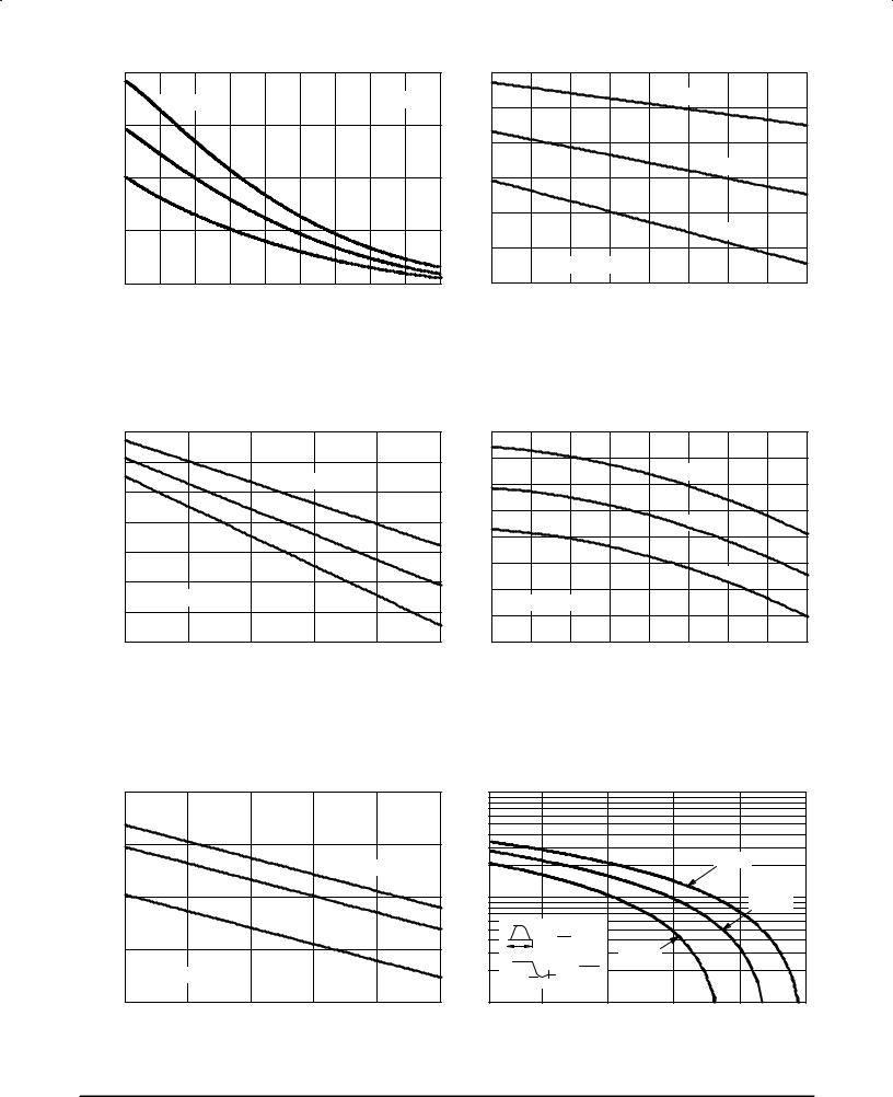
Figure 9.0 Typical Exponential Static dv/dt Versus |
Figure 10.0 Typical Exponential Static dv/dt Versus |
Gate±MT1 Resistance, MT2(+). |
Peak Voltage, MT2(+). |
110 |
|
|
|
|
180 |
100 |
|
|
|
|
160 |
|
|
|
|
|
|
90 |
|
|
VPK = 400V |
|
140 |
|
|
|
|
|
|
80 |
|
|
|
|
120 |
|
|
|
|
|
|
|
|
|
600V |
|
100 |
70 |
|
|
|
|
|
STATICdv/dt(V/S)m |
|
|
|
|
80 |
|
|
800V |
|
(V/dv/dtSTATICS)m |
|
60 |
|
|
|
|
60 |
|
RG ± MT1 = 510W |
|
|
||
50 |
|
|
|
||
|
|
|
|
40 |
|
|
|
|
|
|
|
40 |
105 |
110 |
115 |
120 |
20 |
100 |
125 |
||||
|
|
TJ, Junction Temperature (°C) |
|
|
|
|
|
|
|
TJ = 100°C |
|
|
|
|
|
|
|
|
|
110°C |
|
|
|
|
|
|
|
|
|
120°C |
|
|
|
RG ± MT1 = 510W |
|
|
|
|
|
||
400 |
450 |
500 |
550 |
600 |
650 |
700 |
750 |
800 |
|
|
|
VPK, Peak Voltage |
(Volts) |
|
|
|
|
Figure 11.0 Typical Exponential Static dv/dt Versus |
Figure 12.0 Typical Exponential Static dv/dt Versus |
Junction Temperature, MT2(+) |
Peak Voltage, MT2(±) |
|
|
|
|
|
|
s) |
|
|
|
|
|
|
|
|
|
|
|
|
m |
|
|
|
|
|
|
|
|
|
|
|
|
(V/ |
|
|
|
|
|
|
200 |
|
|
|
|
|
VOLTAGE |
100 |
|
|
|
|
|
|
|
|
|
|
|
|
|
|
|
|
|
|
150 |
|
|
|
|
|
OF COMMUTATING |
|
|
|
|
|
|
|
|
|
|
VPK = 400V |
|
|
|
|
|
90°C |
|
|
|
|
|
600V |
|
|
|
|
|
|
|
||
|
|
|
|
|
|
|
|
|
|
|
||
100 |
|
|
|
|
|
10 |
|
|
|
|
100°C |
|
S)(V/dv/dtm |
|
|
|
|
|
|
|
|
|
|
||
STATIC |
|
|
800V |
|
|
OFRISE |
|
|
1 |
|
|
|
|
|
|
|
|
|
f = 2 tw |
|
|
|
|||
50 |
|
|
|
|
|
|
|
tw |
|
° |
|
|
|
|
|
|
|
|
RATE |
|
|
6f ITM |
110 C |
|
|
|
RG ± MT1 = 510W |
|
|
|
|
(di/dt)c = 1000 |
|
|
|
|||
|
|
|
|
, CRITICAL |
|
VDRM |
|
|
|
|
||
0 |
|
|
|
|
|
1 |
|
|
|
|
|
|
100 |
105 |
110 |
115 |
120 |
125 |
1 |
5 |
10 |
15 |
20 |
25 |
|
|
|
TJ, Junction Temperature (°C) |
|
(di/dt)c, CRITICAL RATE OF CHANGE OF COMMUTATING CURRENT (A/ms) |
||||||||
|
|
|
c |
|||||||||
Figure 13.0 |
Typical Exponential Static dv/dt Versus |
(dv/dt) |
Figure 14.0 |
Critical Rate of Rise of |
|
|
||||||
|
|
Junction Temperature, MT2(±) |
|
|
|
Commutating Voltage |
|
|
||||
|
|
|
|
|
|
|
|
|||||
Data Sheets |
4 |
Motorola Thyristor Device Data |
MAC15S SERIES
|
|
|
|
|
|
|
|
|
|
|
|
|
|
|
|
|
|
|
|
|
|
|
|
|
|
|
|
|
|
|
|
|
|
|
|
|
|
|
|
|
|
|
|
|
|
|
|
|
|
|
|
|
|
|
|
|
|
|
|
|
|
|
|
|
|
20 mHY |
|
|
|
|
|
|
|
1N4007 |
|
|
|
|
|
|
|||
400 VRMS |
|
|
|
|
|
|
|
|
|
|
LL |
|
|
|
|
|
|
|
|
|
|
|
|
|
|
|
|
ADJUST FOR |
|
|
|
|
|
|
|
|
|
|
|
MEASURE |
|
|
15W |
|
|
|
|
|
|
||||||
ITM, 60 Hz VAC |
|
|
|
|
|
|
|
|
|
|
|
|
I |
|
|
|
RS |
|
|
|
|
|
|
||||
|
|
|
|
|
|
|
|
CONTROL |
|
|
|
|
|
|
|
|
|
|
|
|
|
||||||
|
|
|
TRIGGER |
CHARGE |
|
|
|
|
|
|
|
|
|
|
|
|
|
|
|
± |
|
|
|
|
|
||
|
|
|
|
|
|
|
|
|
|
|
|
|
|
|
|
|
|
|
|
|
|
|
|
||||
CHARGE |
CONTROL |
|
|
|
|
|
|
|
|
|
|
CS |
|
|
0.01 mF |
|
|
|
|
400 V |
|||||||
|
|
|
|
|
|
|
|
|
|
|
|
|
+ |
|
|
|
|
||||||||||
|
|
|
|
|
|
|
|
|
|
|
|
|
|
|
|
|
|
|
|||||||||
|
|
|
|
|
|
|
|
|
|
TRIGGER |
|
|
|
2 |
|
|
ADJUST FOR |
|
|
|
|
|
|||||
|
|
|
|
|
|
|
|
|
|
|
|
|
|
|
|
|
|
|
|
||||||||
|
|
|
|
|
|
|
|
|
|
|
|
|
|
|
|
|
|
|
|
|
|
|
|||||
|
|
|
|
NON-POLAR |
|
|
1N914 |
G |
|
|
|
|
dv/dt(c) |
|
|
|
|
|
|
||||||||
|
|
|
|
|
|
|
|
|
|
|
|
|
|
|
|
||||||||||||
|
|
|
|
|
|
1 |
|
|
|
|
|
|
|
|
|
|
|||||||||||
|
|
|
|
|
5 mF |
|
|
|
|
|
|
|
|
|
|
|
|
|
|
|
|
|
|
|
|
||
|
|
|
|
|
|
|
|
|
|
|
|
|
|
|
|
|
|
|
|
|
|
|
|
|
|
|
|
|
|
|
|
|
|
|
|
|
|
|
|
|
|
|
|
|
|
|
|
|
|
|
|
|
|
|
|
|
|
|
|
|
CL |
|
|
|
|
|
|
|
|
|
|
|
|
|
|
|
|
|
|
|
|
||
|
|
|
|
|
|
|
|
|
|
|
|
|
|
|
|
|
|
|
|
|
|
||||||
|
|
|
|
|
|
|
|
|
|
|
|
|
|
|
|
|
|
|
|
|
|
|
|
|
|
||
|
|
|
Note: Component values are for verification of rated (dv/dt)c. See AN1048 for additional information. |
|
|
|
|
|
|
||||||||||||||||||
Figure 15.0 Simplified Test Circuit to Measure the Critical Rate of Rise of Commutating Voltage
Motorola Thyristor Device Data |
5 |
Data Sheets |