Материал: SG6105
Product Specification
Power Supply Supervisor + Regulator + PWM |
SG6105 |
|
|
FEATURES
PC half-bridge (or 494) power supply supervisor + two 431 + PWM
High integration & few external components Over-voltage protection for 3.3V, 5V and 12V Under-voltage protection for 3.3V, 5V and 12V Under-voltage protection for –12V and/or –5V Over-power and short-circuit protection Power-down warning circuitry
Power good circuitry
Delay time for PSON and PG signal Remote ON/OFF function
On-chip oscillator and error amplifier
Two shunt regulator for 3.3V and 5V-Standby Latching PWM for cycle-by-cycle switching Push-pull PWM operation and totem pole outputs Soft-start and maximum 93% duty cycle
APPLICATIONS
Switching mode power supply for Computers, such
as:
ATX |
NLX |
SFX (micro-ATX) |
DESCRIPTION
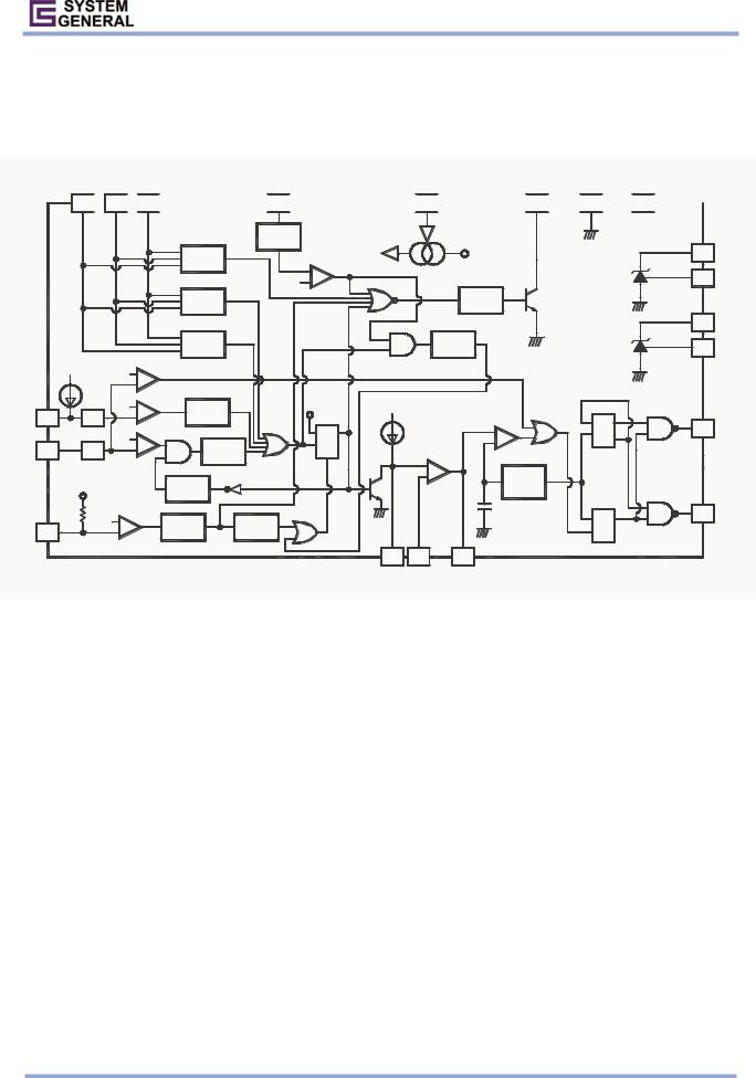
SG6105 controller is designed for switching mode power supply for desktop PCs. It provides all the functions necessary to monitor and control the output of the power supply. Remote ON/OFF control, power good circuitry, some protection features against over-voltage and over-power are implemented. It directly senses all the output rails for OVP without the need of external dividers. An innovated AC-signal sampling circuitry provides a sufficient power-down warning signal for PG. A built-in timer generates accuracy timing for control circuit including the PS-off delay. The cycle-by-cycle PWM switching prevents the power transformer from the saturation and ensures the fastest response for the short-circuit protection which greatly reduce the stress for power transistors. Two internal precision TL431 shunt regulators provide stable reference voltage and driver for 3.3V and 5V-standby regulation. Utilizing minimum number of external components, the SG6105 includes all of the functions for push-pull and/or half-bridge topology, decreasing the production cost and PCB space, and increasing the MTBF for power supply.
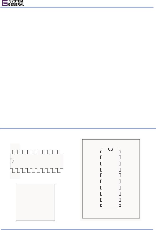
MARKING DIAGRAMS |
PIN CONFIGURATION |
||||
20 |
|
|
|
|
|
|
PSON |
1 |
20 |
VCC |
|
SG6105TP |
V33 |
2 |
19 |
RI |
|
|
|
|
|
||
XXXXXXXYYWWV |
V5 |
3 |
18 |
SS |
|
|
OPP |
4 |
17 |
IN |
|
1 |
UVAC |
5 |
16 |
COMP |
|
|
NVP |
6 |
15 |
GND |
|
T: D = DIP |
V12 |
7 |
14 |
FB1 |
|
OP2 |
8 |
13 |
VREF1 |
||
P : Z = Lead Free |
|||||
|
|
|
|
||
Null=regular package |
OP1 |
9 |
12 |
VREF2 |
|
XXXXXXX: Wafer Lot |
PG |
10 |
11 |
FB2 |
|
YY: Year; WW: Week |
|||||
|
|
|
|
||
V: Assembly Location |
|
|
|
|
|
©System General Corp. |
- 1 - |
www.sg.com.tw |
Version 2.4(IRO33.0011.B1) |
|
Apr.7, 2004 |

|
|
|
|
|
|
Product Specification |
|
|||
Power Supply Supervisor + Regulator + PWM |
SG6105 |
|
||||||||
|
|
|
|
|
|
|
|
|
|
|
ORDERING INFORMATION |
|
|
|
|
|
|
||||
Part Number |
|
Package |
|
|
|
|
|
|||
SG6105D |
|
|
20-Pin DIP |
|
|
|
|
|
|
|
SG6105DZ |
|
|
20-Pin DIP(Lead Free) |
|
|
|
|
|
||
|
|
|
|
|
|
|
||||
PIN DESCRIPTIONS |
|
|
|
|
|
|
||||
|
Name |
Pin |
Type |
Function |
|
|
|
|
||
|
VCC |
20 |
Supply |
Supply voltage. 4.5V ~ 5.5V. It is connected to 5V-standby. |
|
|
|
|
||
|
PG |
10 |
Logic output |
Power Good logic output, 0 or 1 (open-collector). PG = 1 means that the power is good for operation. |
|
|
|
|||
|
The PG delay is 300 msec. |
|
|
|
|
|||||
|
|
|
|
|
|
|
|
|
||
|
V33 |
2 |
Analog input |
3.3V over-voltage/under-voltage control sense input. |
|
|
|
|
||
|
V5 |
3 |
Analog input |
5V over-voltage/under-voltage control sense input. |
|
|
|
|
||
|
V12 |
7 |
Analog input |
12V over-voltage/under-voltage control sense input. |
|
|
|
|
||
|
OPP |
4 |
Analog input |
Over-power sense input. This pin is connected to driver transformer or the output of current |
|
|
|
|||
|
transformer. When not in use, this pin should be grounded. |
|
|
|
|
|||||
|
|
|
|
|
|
|
|
|
||
|
|
|
|
|
Remote On/Off logic input for CPU or controller. Turn on/off the PWM Output after the 7.5 msec / 26 |
|
|
|
||
|
PSON |
1 |
Logic input |
msec delay. |
|
|
|
|
||
|
PSON = 0 means that the main SMPS is operational. |
|
|
|
|
|||||
|
|
|
|
|
|
|
|
|
||
|
|
|
|
|
PSON =1 means that the main SMPS is off and the latch is reset. |
|
|
|
|
|
|
NVP |
6 |
Analog input |
The protection input for negative output, such as –12V and/or –5V. Trip voltage = 2.1V. |
|
|
|
|
||
|
UVAC |
5 |
Analog input |
AC fail detection, detect main AC voltage under-voltage and/or failure. |
|
|
|
|
||
|
COMP |
16 |
Analog output |
Error amplifier output and the input of the PWM comparator. |
|
|
|
|
||
|
IN |
17 |
Analog input |
The negative input of error amplifier. The positive input of error amplifier is a 2.5V reference voltage. |
|
|
|
|||
|
SS |
18 |
Analog input |
The soft-start. It is settable through external capacitor. The current source output at this pin is 8uA and |
|
|
|
|||
|
the voltage is clamped at 2.5V. |
|
|
|
|
|||||
|
|
|
|
|
|
|
|
|
||
|
OP1/OP2 |
9/8 |
Analog output |
The totem-pole output drivers of push-pull PWM. The output are enabled (low) only when the NAND |
|
|
|
|||
|
gate inputs are high, the maximum duty cycle on an output (OP1 or OP2) is 46%. |
|
|
|
|
|||||
|
|
|
|
|
|
|
|
|
||
|
FB1 |
14 |
Analog output |
Output for first converter regulation loop. |
|
|
|
|
||
|
VREF1 |
13 |
Analog input |
Reference comparison input for first converter regulation loop. 2.5V. |
|
|
|
|
||
|
FB2 |
11 |
Analog output |
Output for second converter regulation loop. |
|
|
|
|
||
|
VREF2 |
12 |
Analog input |
Reference comparison input for second converter regulation loop. 2.5V. |
|
|
|
|
||
|
RI |
19 |
Program. |
Connected to external resistor for the reference setting. |
|
|
|
|
||
|
Analog input |
RI = 75k ohms. |
|
|
|
|
||||
|
|
|
|
|
|
|
||||
|
GND |
15 |
Supply |
Ground. |
|
|
|
|
||
©System General Corp. |
- 2 - |
www.sg.com.tw |
Version 2.4(IRO33.0011.B1) |
|
Apr.7, 2004 |
Product Specification
Power Supply Supervisor + Regulator + PWM |
SG6105 |
|
|
BLOCK DIAGRAM
V33 |
V5 |
V12 |
UVAC |
RI |
PG |
GND |
VCC |
2 
 3
3 
 7
7 
 5
5 
 19
19 
 10
10 
 15
15 
 20
20 
|
|
|
|
|
|
|
DSD |
|
|
|
|
|
|
|
|
|
|
|
|
|
|
|
|
UV |
|
|
|
2uA |
|
Vref |
|
|
|
14 |
FB1 |
|
|
|
|
|
|
Detector |
|
_ |
COMP |
|
|
|
|
|
|
|
|
|
|
|
|
|
|
|
|
|
|
|
|
|
13 |
VREF1 |
|||
|
|
|
|
|
|
|
0.7V |
+ |
|
|
|
|
|
|
|
||
|
|
|
|
|
|
|
|
|
|
|
|
|
|
|
|
||
|
|
|
|
|
|
OV |
|
|
|
|
|
Delay |
|
|
|
|
|
|
|
|
|
|
|
Protector |
|
|
|
|
|
300msec |
|
|
|
|
|
|
|
|
|
|
|
|
|
|
|
|
|
|
|
|
|
11 |
FB2 |
|
|
|
|
|
|
UV |
|
|
|
|
|
Delay |
|
|
|
12 |
VREF2 |
|
|
|
|
|
|
Protector |
|
|
|
|
|
3sec |
|
|
|
||
|
|
5V |
3.2V |
_ |
COMP |
|
|
|
|
|
|
|
|
|
|
|
|
|
|
|
|
|
|
|
|
|
|
|
|
|
|
|
|
|
|
|
|
|
|
+ |
|
|
|
|
|
|
|
|
|
|
|
|
|
|
|
64uA |
2.1V |
_ |
COMP |
|
|
|
|
|
|
|
|
|
|
|
|
|
|
|
|
Vcc |
|
2.5V |
|
|
|
|
|
|
|
||||
|
|
|
|
|
Delay |
|
|
|
|
|
|
|
|
|
|||
NVP |
6 |
Buffer |
|
+ |
|
7msec |
|
|
|
|
|
|
|
D |
Q |
|
|
|
|
|
|
|
|
|
|
|
|
9 |
OP1 |
||||||
|
|
|
|
|
|
|
|
|
|
|
|
|
|
||||
|
|
|
2.4V |
_ |
COMP |
|
|
D |
Q |
8uA |
|
_ |
CK |
_ |
|||
|
|
|
|
|
|
|
|
CK |
|
|
|
+ |
|
Q |
|
|
|
OPP |
4 |
Buffer |
|
+ |
|
Delay |
|
|
|
|
|
COMP |
|
|
|
||
|
|
|
|
R |
|
|
|
|
|
|
|
||||||
|
|
7msec |
|
|
|
|
|
|
|
|
|
||||||
|
|
|
|
|
|
|
|
|
|
|
|
+ |
|
|
|
|
|
|
|
|
|
|
|
|
|
|
|
|
|
_ |
|
O.S.C |
|
|
|
|
|
Vcc |
|
|
|
Delay |
|
|
|
|
|
Error |
|
|
|
|
|
|
|
|
|
|
|
15msec |
|
|
|
|
|
Amp |
|
|
|
|
|
|
|
1.4V |
_ |
COMP |
On/Off Delay |
|
|
|
|
|
|
|
S |
Q |
8 |
OP2 |
|
|
|
Delay |
|
|
|
|
|
|
|
|
|||||||
|
|
|
|
|
|
26msec |
|
|
|
|
|
|
|
|
|
|
|
PSON |
1 |
|
+ |
|
|
2msec |
|
|
|
|
|
|
R |
|
|
|
|
|
|
|
7.5msec |
|
|
|
|
|
|
|
|
|
|||||
|
|
|
|
|
|
|
|
|
|
|
|
|
|||||
|
|
|
|
|
|
|
|
|
|
18 |
17 |
16 |
|
|
|
|
|
|
|
|
|
|
|
|
|
|
|
SS |
IN |
COMP |
|
|
|
|
|
©System General Corp. |
- 3 - |
www.sg.com.tw |
Version 2.4(IRO33.0011.B1) |
|
Apr.7, 2004 |
Product Specification
Power Supply Supervisor + Regulator + PWM |
SG6105 |
|
|
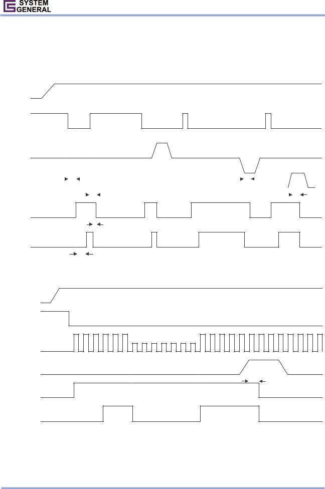
TIMING DIAGRAM
VCC
PSON
3.3V,5V,12V
NVP |
tPSON(ON) |
|
|
|
|
tUVP |
|
|
|
|
|
||||
|
|
|
|
|
|
|
|
|
|||||||
|
|
|
|
|
|
|
|
|
|
|
|
|
|
|
|
|
|
|
|
|
|
|
tPSON(OFF) |
|
|
|
|
tNVP |
|
|
|
|
|
|
|
|
|
|
|
|
|
|
|
|
|
||
SS(on/off)
tPSOFF
PG
tPG
VCC
PSON
Voltage < VUVAC
UVAC
OPP
tOPP
SS(on/off)
PG
©System General Corp. |
- 4 - |
www.sg.com.tw |
Version 2.4(IRO33.0011.B1) |
|
Apr.7, 2004 |

|
|
|
Product Specification |
|||
Power Supply Supervisor + Regulator + PWM |
|
|
SG6105 |
|||
|
|
|
|
|
|
|
ABSOLUTE MAXIMUM RATINGS |
|
|
|
|
|
|
Symbol |
Parameter |
Value |
|
Unit |
|
|
VCC |
DC Supply Voltage at Pin 20 |
16 |
|
V |
|
|
VFB |
Shunt Regulator Output at Fb1, Fb2 Pins |
16 |
|
V |
|
|
IOUT |
Output Current at PG, Fb1, Fb2 Pins |
30 |
|
mA |
|
|
PD,25 |
Power Dissipation (TA=25 ) |
1.5 |
|
W |
|
|
PD,90 |
Power Dissipation (TA=90 ) |
0.5 |
|
W |
|
|
TSTG |
Storage Temperature Range |
-55 to +150 |
|
|
|
|
RθJA |
Thermal Resistance, Junction-To-Air |
82.5 |
|
/W |
|
|
TJ,MAX |
Operating Junction Temperature |
150 |
|
|
|
|
TA,MAX |
Operating Ambient Temperature |
-30 to +125 |
|
|
|
|
TL |
Lead Temperature (Soldering, 10sec) |
260 |
|
|
|
|
|
ESD Capability, HBM model |
3.0 |
|
kV |
|
|
Note: All voltage values, except differential voltage, are with respect to network ground terminal.
RECOMMENDED OPERATING CONDITIONS
Symbol |
Parameter |
Value |
Unit |
|
VCC |
DC Supply Voltage at Pin 20 |
4.5 to 5.5 |
V |
|
VFB |
Shunt Regulator Output at Fb1, Fb2 Pins |
4 to 16 |
V |
|
TOPER |
Operating Ambient Temperature Range |
-25 to +85 |
|
|
|
|
|
|
|
ELECTRICAL CHARACTERISTICS (VCC = 5V, TA = 25°C)
Symbol |
Parameter |
Test Condition |
Min. |
Typ. |
Max. |
Unit |
ICC |
Total Supply Current |
PG High |
- |
5 |
10 |
mA |
VOVP1 |
Over-Voltage Protection 3.3V |
- |
3.9 |
4.1 |
4.3 |
V |
VOVP2 |
Over-Voltage Protection 5V |
- |
5.8 |
6.1 |
6.5 |
V |
VOVP3 |
Over-Voltage Protection 12V |
- |
13.9 |
14.5 |
14.9 |
V |
VUVP1 |
Under-Voltage Protection 3.3V |
- |
2.0 |
2.6 |
2.8 |
V |
VUVP2 |
Under-Voltage Protection 5V |
- |
3.0 |
3.6 |
3.9 |
V |
VUVP3 |
Under-Voltage Protection 12V |
- |
6.0 |
7.2 |
8.0 |
V |
VUVS1 |
Under-Voltage Sense 3.3V for PG Low |
- |
2.5 |
2.8 |
3.0 |
V |
VUVS2 |
Under-Voltage Sense 5V for PG Low |
- |
4.0 |
4.3 |
4.5 |
V |
VUVS3 |
Under-Voltage Sense 12V for PG Low |
- |
9.4 |
10.1 |
10.4 |
V |
VOPPS* 1 |
Over-Power Protection. |
VUVAC = 1.5V |
2.02 |
2.4 |
2.66 |
V |
VNVP |
Negative Voltage Protection: Voltage Level |
- |
2.0 |
2.1 |
2.2 |
V |
INVP |
Negative Voltage Protection: Source Current |
RI = 75kΩ |
57 |
64 |
72 |
uA |
tOVP |
Timing for Over-Voltage Protection |
RI = 75kΩ |
0.37 |
0.7 |
1.35 |
ms |
tUVP |
Timing for Under-Voltage Protection |
RI = 75kΩ |
0.8 |
2.4 |
3.75 |
ms |
tUVS |
Timing for Under-Voltage Sense for PG Low |
RI = 75kΩ |
0.37 |
1.2 |
1.88 |
ms |
tOPP |
Timing for Over-Power-Protection |
RI = 75kΩ |
3.3 |
7 |
11.3 |
ms |
tNVP |
Timing for Negative Voltage Protection |
RI = 75kΩ |
3.3 |
7 |
10.2 |
ms |
Note *1: VOPPS = (2/3) x VOPP + (1/3) x VUVAC ;
©System General Corp. |
- 5 - |
www.sg.com.tw |
Version 2.4(IRO33.0011.B1) |
|
Apr.7, 2004 |