Материал: mhpm7b16a120brev0
MOTOROLA
SEMICONDUCTOR TECHNICAL DATA
Order this document by MHPM7B16A120B/D
Hybrid Power Module
Integrated Power Stage for 3.0 hp Motor Drives
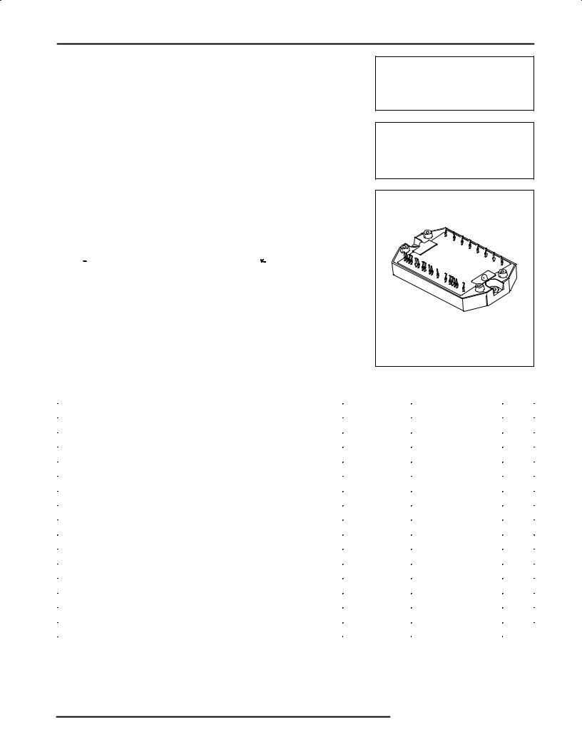
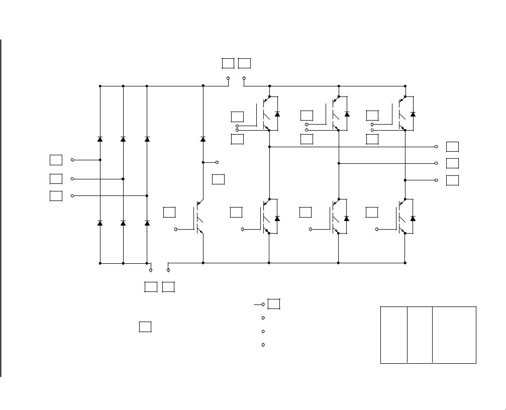
This module integrates a 3±phase input rectifier bridge, 3±phase output inverter and brake transistor/diode in a single convenient package. The output inverter utilizes advanced insulated gate bipolar transistors (IGBT) matched with free±wheeling diodes to give optimal dynamic performance. It has been configured for use as a three±phase motor drive module or for many other power switching applications. The top connector pins have been designed for easy interfacing to the user's control board.
•Short Circuit Rated 10 μs @ 25°C
•Pin-to-Baseplate Isolation Exceeds 2500 Vac (rms)
•Convenient Package Outline
•UL Recognized and Designed to Meet VDE
•Access to Positive and Negative DC Bus
MHPM7B16A120B
Motorola Preferred Device
16 AMP, 1200 VOLT
HYBRID POWER MODULE
PLASTIC PACKAGE |
|
CASE 440A±01, Style |
1 |
MAXIMUM DEVICE RATINGS (TJ = 25°C unless otherwise noted)
Rating |
Symbol |
Value |
Unit |
|
|
|
|
INPUT RECTIFIER BRIDGE |
|
|
|
|
|
|
|
Repetitive Peak Reverse Voltage |
VRRM |
1200 |
V |
Average Output Rectified Current (1) |
IO |
16 |
A |
Peak Non-repetitive Surge Current |
IFSM |
330 |
A |
OUTPUT INVERTER |
|
|
|
|
|
|
|
IGBT Reverse Voltage |
VCES |
1200 |
V |
Gate-Emitter Voltage |
VGES |
± 20 |
V |
Continuous IGBT Collector Current |
IC |
16 |
A |
Peak IGBT Collector Current ± (PW = 1.0 ms) (2) |
IC(pk) |
32 |
A |
Continuous Free-Wheeling Diode Current |
IF |
16 |
A |
Peak Free-Wheeling Diode Current ± (PW = 1.0 ms) (2) |
IF(pk) |
32 |
A |
IGBT Power Dissipation |
PD |
75 |
W |
Free-Wheeling Diode Power Dissipation |
PD |
40 |
W |
IGBT Junction Temperature Range |
TJ |
± 40 to +125 |
°C |
Free-Wheeling Diode Junction Temperature Range |
TJ |
± 40 to +125 |
°C |
(1) 1 cycle = 50 or 60 Hz
(2) 1 ms = 1.0% duty cycle
Preferred devices are Motorola recommended choices for future use and best overall value.
Motorola, Inc. 1995
MOTOROLA
1

MAXIMUM DEVICE RATINGS (continued) (TJ = 25°C unless otherwise noted)
Rating |
Symbol |
Value |
Unit |
|
|
|
|
BRAKE CIRCUIT |
|
|
|
|
|
|
|
IGBT Reverse Voltage |
VCES |
1200 |
V |
Gate-Emitter Voltage |
VGES |
± 20 |
V |
Continuous IGBT Collector Current |
IC |
16 |
A |
Peak IGBT Collector Current (PW = 1.0 ms) (2) |
IC(pk) |
32 |
A |
IGBT Power Dissipation |
PD |
75 |
W |
|
|
|
|
Diode Reverse Voltage |
VRRM |
1200 |
V |
Continuous Output Diode Current |
IF |
16 |
A |
Peak Output Diode Current (PW = 1.0 ms) (2) |
IF(pk) |
32 |
A |
TOTAL MODULE |
|
|
|
|
|
|
|
Isolation Voltage ± (47±63 Hz, 1.0 Minute Duration) |
VISO |
2500 |
VAC |
Ambient Operating Temperature Range |
TA |
± 40 to + 85 |
°C |
Operating Case Temperature Range |
TC |
± 40 to + 90 |
°C |
Storage Temperature Range |
Tstg |
± 40 to +150 |
°C |
Mounting Torque |
± |
6.0 |
lb±in |
|
|
|
|
ELECTRICAL CHARACTERISTICS (TJ = 25°C unless otherwise noted)
Characteristic |
Symbol |
Min |
Typ |
Max |
Unit |
|
|
|
|
|
|
INPUT RECTIFIER BRIDGE |
|
|
|
|
|
|
|
|
|
|
|
Reverse Leakage Current (VRRM = 1200 V) |
IR |
± |
10 |
50 |
μA |
Forward Voltage (IF = 16 A) |
VF |
± |
1.05 |
1.5 |
V |
Thermal Resistance (Each Die) |
RθJC |
± |
± |
2.7 |
°C/W |
OUTPUT INVERTER |
|
|
|
|
|
|
|
|
|
|
|
Gate-Emitter Leakage Current (VCE = 0 V, VGE = ± 20 V) |
IGES |
± |
± |
± 20 |
μA |
Collector-Emitter Leakage Current (VCE = 1200 V, VGE = 0 V) |
ICES |
|
|
|
|
TJ = 25°C |
|
± |
± |
100 |
μA |
TJ = 125°C |
|
± |
± |
2.0 |
mA |
Gate-Emitter Threshold Voltage (VCE = VGE, IC = 10 mA) |
VGE(th) |
4.0 |
6.0 |
8.0 |
V |
Collector-Emitter Breakdown Voltage (IC = 10 mA, VGE = 0) |
V(BR)CES |
1200 |
1300 |
± |
V |
Collector-Emitter Saturation Voltage (IC = 16 A, VGE = 15 V) |
VCE(SAT) |
± |
2.4 |
3.5 |
V |
Input Capacitance (VGE = 0 V, VCE = 10 V, f = 1.0 MHz) |
Cies |
± |
2700 |
± |
pF |
Input Gate Charge (VCE = 600 V, IC = 16 A, VGE = 15 V) |
QT |
± |
100 |
± |
nC |
Fall Time ± Inductive Load |
tfi |
|
|
|
|
(VCE = 600 V, IC = 16 A, VGE = 15 V, RG = 150 Ω) |
|
± |
350 |
500 |
ns |
Turn-On Energy |
E(on) |
± |
± |
2.5 |
mJ |
(VCE = 600 V, IC = 16 A, VGE = 15 V, RG = 150 Ω) |
|
|
|
|
|
Turn-Off Energy |
E(off) |
± |
± |
2.5 |
mJ |
(VCE = 600 V, IC = 16 A, VGE = 15 V, RG = 150 Ω) |
|
|
|
|
|
Diode Forward Voltage (IF = 16 A, VGE = 0 V) |
VF |
± |
1.7 |
2.2 |
V |
Diode Reverse Recovery Time |
trr |
|
|
|
|
(IF = 16 A, V = 600 V, dI/dt = 100 A/μs) |
|
± |
170 |
200 |
ns |
Diode Stored Charge (IF = 16 A, V = 400 V, di/dt = 100 A/μs) |
Qrr |
± |
850 |
1000 |
nC |
Thermal Resistance ± IGBT (Each Die) |
RθJC |
± |
± |
1.4 |
°C/W |
Thermal Resistance ± Free-Wheeling Diode (Each Die) |
RθJC |
± |
± |
2.7 |
°C/W |
(2) 1.0 ms = 1.0% duty cycle |
|
|
|
|
|
MHPM7B16A120B |
MOTOROLA |
2 |
|

ELECTRICAL CHARACTERISTICS (continued) (TJ = 25°C unless otherwise noted)
Characteristic |
Symbol |
Min |
Typ |
Max |
Unit |
|
|
|
|
|
|
BRAKE CIRCUIT |
|
|
|
|
|
|
|
|
|
|
|
Gate-Emitter Leakage Current (VCE = 0 V, VGE = ± 20 V) |
IGES |
± |
± |
± 20 |
μA |
Collector-Emitter Leakage Current (VCE = 1200 V, VGE = 0 V) |
ICES |
|
|
|
|
TJ = 25°C |
|
± |
± |
100 |
μA |
TJ = 125°C |
|
± |
± |
2.0 |
mA |
Gate-Emitter Threshold Voltage (VCE = VGE, IC = 10 mA) |
VGE(th) |
4.0 |
6.0 |
8.0 |
V |
Collector-Emitter Breakdown Voltage (IC = 10 mA, VGE = 0) |
V(BR)CES |
1200 |
1300 |
± |
V |
Collector-Emitter Saturation Voltage (VGE = 15 V, IC = 16 A) |
VCE(SAT) |
± |
2.4 |
3.5 |
V |
Input Capacitance (VGE = 0 V, VCE = 10 V, f = 1.0 MHz) |
Cies |
± |
2700 |
± |
pF |
Input Gate Charge (VCE = 600 V, IC = 16 A, VGE = 15 V) |
QT |
± |
100 |
± |
nC |
Fall Time ± Inductive Load |
tfi |
|
|
|
|
(VCE = 600 V, IC = 16 A, VGE = 15 V, RG = 150 Ω) |
|
± |
350 |
500 |
ns |
Turn-On Energy |
E(on) |
|
|
|
|
(VCE = 600 V, IC = 16 A, VGE = 15 V, RG = 150 Ω) |
|
± |
± |
2.5 |
mJ |
Turn-Off Energy |
E(off) |
|
|
|
|
(VCE = 600 V, IC = 16 A, VGE = 15 V, RG = 150 Ω) |
|
± |
± |
2.5 |
mJ |
Diode Forward Voltage (IF = 16 A) |
VF |
± |
1.7 |
2.2 |
V |
Diode Reverse Leakage Current (VR = 1200 V) |
IR |
± |
± |
50 |
μA |
Thermal Resistance ± IGBT |
RθJC |
± |
± |
1.4 |
°C/W |
Thermal Resistance ± Diode |
RθJC |
± |
± |
2.7 |
°C/W |
MOTOROLA |
MHPM7B16A120B |
|
3 |
4 |
MHPM7B16A120B |
Schematic Stage Power Integrated .1 Figure
MOTOROLA
|
|
|
1 |
7 |
|
|
|
|
|
|
|
|
|
P1 |
P2 |
|
|
|
|
|
|
|
|
|
|
|
Q1 |
|
Q3 |
|
Q5 |
|
|
|
|
9 |
|
D1 |
11 |
D3 |
13 |
D5 |
|
|
|
|
|
|
|
|
|
|||
|
|
|
|
|
|
|
|
|
|
|
|
|
|
G1 |
|
|
G3 |
|
G5 |
|
|
|
|
|
E1 |
|
|
E3 |
|
E5 |
|
|
|
|
|
8 |
|
|
10 |
|
12 |
|
|
|
|
|
|
|
|
|
|
|
U |
20 |
24 |
R |
|
|
|
|
|
|
|
V |
19 |
|
|
|
B |
|
|
|
|
|
||
|
|
|
|
|
|
|
|
|
|
|
23 |
S |
|
21 |
|
|
|
|
|
W |
18 |
22 |
T |
|
Q7 |
|
Q2 |
|
Q4 |
|
Q6 |
|
|
|
|
|
|
|
|||||
|
|
15 |
16 |
|
D2 |
17 |
D4 |
14 |
D6 |
|
|
|
|
|
|
|
|
|
|||
|
|
G7 |
G2 |
|
|
G4 |
|
G6 |
|
|
|
N1 |
N2 |
|
|
|
|
|
|
|
|
|
25 |
6 |
|
|
|
|
|
|
|
|
|
|
|
|
NC |
2 |
|
|
|
DEVICE INTEGRATION |
|
|
|
|
|
|
|
|
|
|
||
NC |
|
|
3 |
These pins are physical |
|
|
|
|
|
|
|
||||
= PIN NUMBER IDENTIFICATION |
|
terminations but not |
3±Phase |
Brake |
3±Phase |
||
|
|||||||
NC |
|
|
4 |
connected internally. |
Input |
Output |
|
|
|
IGBT/ |
|||||
|
|
|
|
|
Rectifier |
IGBT/Diode |
|
|
|
|
|
|
Diode |
||
NC |
|
|
5 |
|
Bridge |
Bridge |
|
|
|
|
|
||||
|
|
|
|
|
|
|
|
|
|
|
|
|
Typical Characteristics |
|
|
|
|
||||
|
50 |
TJ = 25°C |
|
VGE = 18 V |
15 V |
|
|
50 |
TJ = 125°C |
|
VGE = 18 V |
15 V |
|
|
45 |
|
|
12 V |
45 |
|
|
||||||
|
|
|
|
|
|
|
|
|
|
|
|||
(A) |
40 |
|
|
|
|
|
(A) |
40 |
|
|
|
|
12 V |
CURRENT |
35 |
|
|
|
|
|
CURRENT |
35 |
|
|
|
|
|
30 |
|
|
|
|
|
30 |
|
|
|
|
|
||
|
|
|
|
|
|
|
|
|
|
|
|
||
, COLLECTOR |
25 |
|
|
|
|
|
, COLLECTOR |
25 |
|
|
|
|
|
20 |
|
|
|
|
|
20 |
|
|
|
|
|
||
15 |
|
|
|
|
9 V |
15 |
|
|
|
|
9 V |
||
10 |
|
|
|
|
10 |
|
|
|
|
|
|||
C |
|
|
|
|
|
C |
|
|
|
|
|
||
I |
|
|
|
|
|
I |
|
|
|
|
|
||
|
5 |
|
|
|
|
|
|
5 |
|
|
|
|
|
|
0 |
|
|
|
|
|
|
0 |
|
|
|
|
|
|
0 |
1 |
2 |
3 |
4 |
|
5 |
0 |
1 |
2 |
3 |
4 |
5 |
|
|
VCE, COLLECTOR±EMITTER VOLTAGE (V) |
|
|
|
VCE, COLLECTOR±EMITTER VOLTAGE (V) |
|
||||||
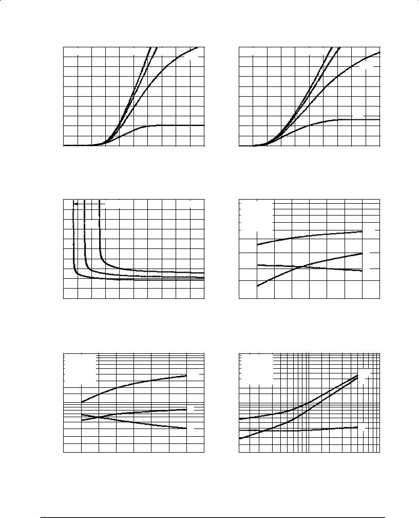
Figure 2. Output Inverter Collector Current IC |
Figure 3. Output Inverter Collector Current IC |
versus Collector±Emitter Voltage VCE |
versus Collector±Emitter Voltage VCE |
(V) |
10 |
|
IC = 8 A |
|
|
TJ = 25°C |
|
1000 |
|
|
|
|
|
|
|
|
|
|
|
|
|
|
V |
CE |
= 600 V |
|
|
|
|
|
|
|
|||
COLLECTOR±EMITTERVOLTAGE |
|
|
|
|
|
|
|
|
|
|
|
|
|
|
|
|
|
8 |
|
|
|
|
|
|
VGE = 15 V |
|
|
|
|
|
|
|
|||
16 A |
|
|
|
|
|
RG = 10 Ω |
|
|
|
|
|
|
|
||||
|
|
|
|
|
TIMESWITCHING(ns) |
TJ = 25°C |
|
|
|
|
|
t(off) |
|
||||
|
|
|
|
|
|
|
|
|
|
|
|
||||||
2 |
|
32 A |
|
|
|
|
|
|
|
|
|
|
|
|
|||
|
|
|
|
|
|
|
|
|
|
|
|
|
|
||||
|
6 |
|
|
|
|
|
|
|
|
|
|
|
|
|
|
|
|
|
|
|
|
|
|
|
|
|
|
|
|
|
|
|
|
|
|
|
4 |
|
|
|
|
|
|
|
|
|
|
|
|
|
|
tf |
|
|
|
|
|
|
|
|
|
|
|
|
|
|
|
|
|
|
|
|
|
|
|
|
|
|
|
|
|
|
|
|
|
|
|
td |
|
, |
|
|
|
|
|
|
|
|
|
|
|
|
|
|
|
|
|
CE |
|
|
|
|
|
|
|
|
|
|
|
|
|
|
|
|
|
V |
|
|
|
|
|
|
|
|
|
|
|
|
|
|
|
|
|
|
0 |
10 |
12 |
14 |
16 |
18 |
|
100 |
|
4 |
6 |
8 |
10 |
12 |
14 |
16 |
18 |
|
8 |
|
2 |
|
|||||||||||||
|
|
|
VGE, GATE±EMITTER VOLTAGE (V) |
|
|
|
|
|
|
|
IC, COLLECTOR CURRENT (A) |
|
|
|
|||
SWITCHING TIME (ns)
Figure 4. Inverter Collector±Emitter Voltage VCE |
|
|
Figure 5. Inverter Switching Time td, tf, t(off) |
|||||||||
|
versus Gate±Emitter Voltage VGE |
|
|
|
|
versus Collector Current IC |
|
|||||
10000 |
VCE = 600 V |
|
|
|
|
|
|
|
|
10000 |
VCE = 600 V |
|
|
|
|
|
|
|
|
|
|
|
|
||
|
VGE = 15 V |
|
|
|
|
|
|
|
|
|
VGE = 15 V |
t(off) |
|
RG = 10 Ω |
|
|
|
|
|
t(off) |
|
|
|
IC = 16 A |
|
|
TJ = 125°C |
|
|
|
|
|
|
|
TIME (ns) |
|
TJ = 25°C |
td |
|
|
|
|
|
|
|
|
|
|
|
|
|
1000 |
|
|
|
|
|
|
|
|
SWITCHING |
1000 |
|
|
|
|
|
|
|
|
|
|
|
|
|
||
|
|
|
|
|
|
|
tf |
|
|
|
|
|
|
|
|
|
|
|
|
td |
|
|
|
|
tf |
100 |
|
|
|
|
|
14 |
16 |
|
|
100 |
|
|
2 |
4 |
6 |
8 |
10 |
12 |
18 |
|
10 |
100 |
1000 |
||
|
|
|
IC, COLLECTOR CURRENT (A) |
|
|
|
|
|
RG, GATE RESISTANCE (Ω) |
|
||
Figure 6. Inverter Switching Time td, tf, t(off)
versus Collector Current IC
Figure 7. Inverter Switching Time td, tf, t(off)
versus Gate Resistance RG
MOTOROLA |
MHPM7B16A120B |
|
5 |