Материал: mur190erev1dx
MOTOROLA
SEMICONDUCTOR TECHNICAL DATA
Order this document by MUR190E/D
SWITCHMODE Power Rectifiers
Ultrafast ªE'' Series with High Reverse Energy Capability
. . . designed for use in switching power supplies, inverters and as free wheeling diodes, these state±of±the±art devices have the following features:
•20 mjoules Avalanche Energy Guaranteed
•Excellent Protection Against Voltage Transients in Switching Inductive Load Circuits
•Ultrafast 75 Nanosecond Recovery Time
•175°C Operating Junction Temperature
•Low Forward Voltage
•Low Leakage Current
•High Temperature Glass Passivated Junction
•Reverse Voltage to 1000 Volts
Mechanical Characteristics:
• Case: Epoxy, Molded
• Weight: 0.4 gram (approximately)
•Finish: All External Surfaces Corrosion Resistant and Terminal Leads are Readily Solderable
•Lead and Mounting Surface Temperature for Soldering Purposes: 220°C Max. for 10 Seconds, 1/16″ from case
•Shipped in plastic bags, 1000 per bag
•Available Tape and Reeled, 5000 per reel, by adding a ªRL'' suffix to the part number
•Polarity: Cathode Indicated by Polarity Band
•Marking: U190E, U1100E
MAXIMUM RATINGS
MUR190E
MUR1100E
MUR1100E is a Motorola Preferred Device
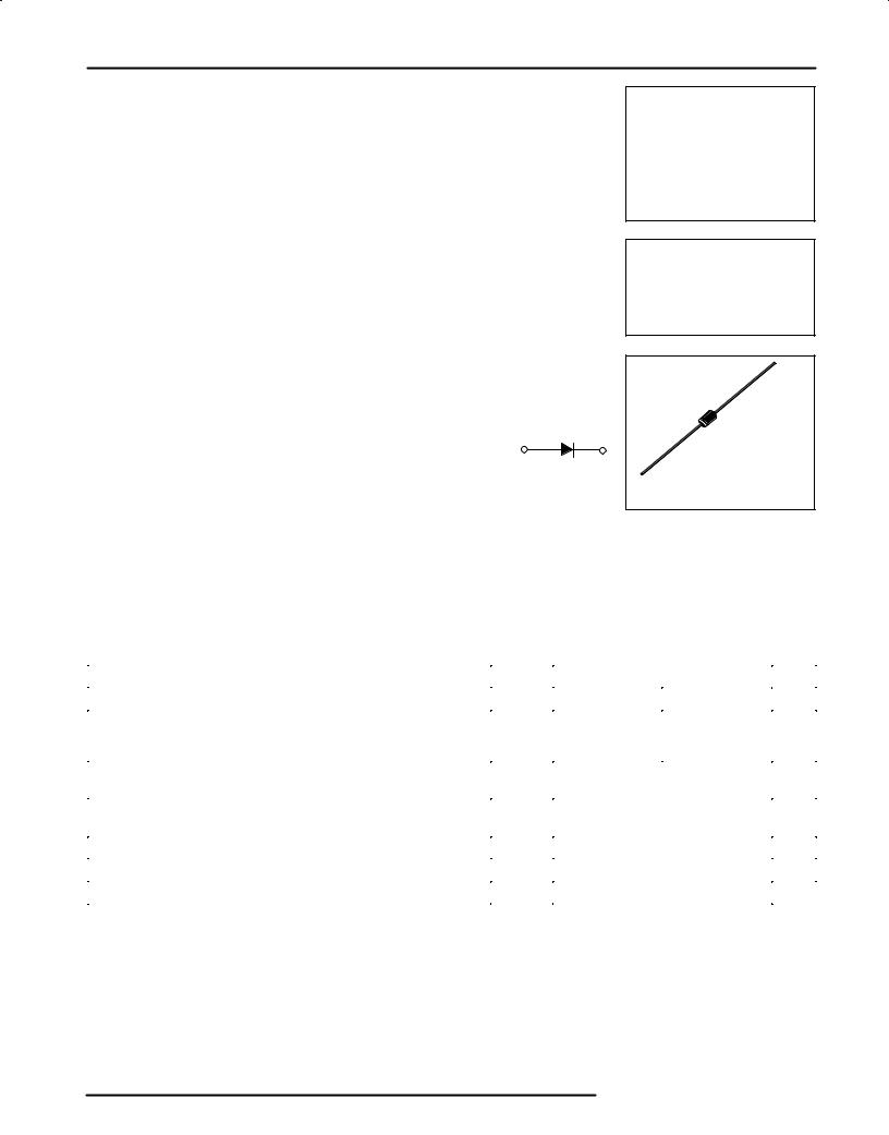
ULTRAFAST
RECTIFIERS
1.0 AMPERE
900±1000 VOLTS
CASE 59±04
|
|
|
MUR |
|
|
Rating |
Symbol |
|
|
|
Unit |
190E |
|
1100E |
|||
|
|
|
|
|
|
Peak Repetitive Reverse Voltage |
VRRM |
900 |
|
1000 |
Volts |
Working Peak Reverse Voltage |
VRWM |
|
|
|
|
DC Blocking Voltage |
VR |
|
|
|
|
Average Rectified Forward Current (Square Wave) |
IF(AV) |
1.0 @ TA = 95°C |
Amps |
||
(Mounting Method #3 Per Note 1) |
|
|
|
|
|
|
|
|
|
|
|
Nonrepetitive Peak Surge Current |
IFSM |
|
35 |
Amps |
|
(Surge applied at rated load conditions, halfwave, single phase, 60 Hz) |
|
|
|
|
|
|
|
|
|
|
|
Operating Junction Temperature and Storage Temperature |
TJ, Tstg |
|
65 to +175 |
°C |
|
THERMAL CHARACTERISTICS |
|
|
|
|
|
|
|
|
|
|
|
Maximum Thermal Resistance, Junction to Ambient |
RθJA |
|
See Note 1 |
°C/W |
|
(1) Pulse Test: Pulse Width = 300 μs, Duty Cycle ≤ 2.0%. |
|
|
|
|
|
SWITCHMODE is a trademark of Motorola, Inc.
Preferred devices are Motorola recommended choices for future use and best overall value.
Rev 1
Rectifier Device Data
Motorola, Inc. 1996

MUR190E MUR1100E
ELECTRICAL CHARACTERISTICS
|
|
|
|
MUR |
|
|
|
Rating |
Symbol |
|
|
|
Unit |
|
190E |
|
1100E |
|||
|
|
|
|
|
|
|
Maximum Instantaneous Forward Voltage (1) |
vF |
|
|
|
Volts |
|
(iF = 1.0 Amp, TJ = 150°C) |
|
|
1.50 |
|
||
(iF = 1.0 Amp, TJ = 25°C) |
|
|
1.75 |
|
||
Maximum Instantaneous Reverse Current (1) |
iR |
|
|
|
μA |
|
(Rated dc Voltage, TJ = 100°C) |
|
|
600 |
|
||
(Rated dc Voltage, TJ = 25°C) |
|
|
10 |
|
||
Maximum Reverse Recovery Time |
trr |
|
|
|
ns |
|
(IF = 1.0 |
Amp, di/dt = 50 Amp/μs) |
|
|
100 |
|
|
(IF = 0.5 |
Amp, iR = 1.0 Amp, IREC = 0.25 Amp) |
|
|
75 |
|
|
Maximum Forward Recovery Time |
tfr |
|
75 |
ns |
||
(IF = 1.0 |
Amp, di/dt = 100 Amp/μs, Recovery to 1.0 V) |
|
|
|
|
|
Controlled Avalanche Energy (See Test Circuit in Figure 6) |
WAVAL |
|
10 |
mJ |
||
(1) Pulse Test: Pulse Width = 300 μs, Duty Cycle ≤ 2.0%.
2 |
Rectifier Device Data |
MUR190E MUR1100E
ELECTRICAL CHARACTERISTICS
|
20 |
|
|
|
|
|
|
|
|
|
|
|
|
10 |
|
|
|
|
|
|
|
|
|
|
|
|
7.0 |
|
|
|
|
|
|
|
|
|
|
|
(AMPS) |
5.0 |
|
|
|
|
|
|
|
|
|
|
|
3.0 |
|
T |
|
= 175°C |
|
|
° |
|
|
|
||
|
|
|
|
|
|
|
|
|||||
|
|
|
J |
|
|
|
|
|
||||
|
2.0 |
|
|
|
|
|
|
25 C |
|
|
|
|
CURRENT |
|
|
|
|
|
|
|
|
|
|
|
|
|
|
|
|
|
|
|
100°C |
|
|
|
||
|
|
|
|
|
|
|
|
|
|
|
||
FORWARD |
1.0 |
|
|
|
|
|
|
|
|
|
|
|
0.7 |
|
|
|
|
|
|
|
|
|
|
|
|
|
|
|
|
|
|
|
|
|
|
|
|
|
INSTANTANEOUS, |
0.5 |
|
|
|
|
|
|
|
|
|
|
|
0.3 |
|
|
|
|
|
|
|
|
|
|
|
|
|
|
|
|
|
|
|
|
|
|
|
|
|
|
0.2 |
|
|
|
|
|
|
|
|
|
|
|
F |
|
|
|
|
|
|
|
|
|
|
|
|
i |
|
|
|
|
|
|
|
|
|
|
|
|
|
0.1 |
|
|
|
|
|
|
|
|
|
|
|
|
0.07 |
|
|
|
|
|
|
|
|
|
|
|
|
0.05 |
|
|
|
|
|
|
|
|
|
|
|
|
0.03 |
|
|
|
|
|
|
|
|
|
|
|
|
0.02 |
|
|
|
|
|
|
|
|
|
|
|
|
0.01 |
|
|
|
|
|
|
|
|
|
|
|
|
0.3 |
0.5 |
0.7 |
|
0.9 |
1.1 |
1.3 |
1.5 |
1.7 |
1.9 |
2.1 |
2.3 |
vF, INSTANTANEOUS VOLTAGE (VOLTS)
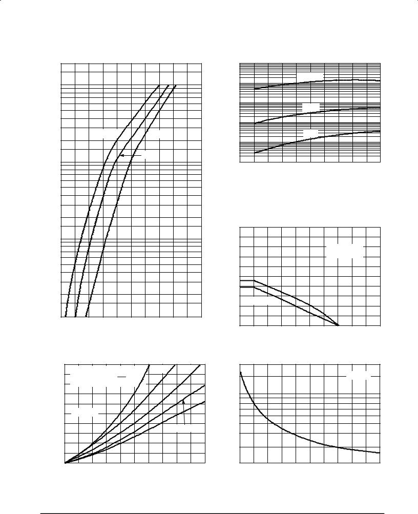
Figure 1. Typical Forward Voltage
(WATTS) |
5.0 |
(CAPACITIVE LOAD) IPK + 20 |
10 |
5.0 |
|
|
|
|
|||||
|
|
|
|
|||
DISSIPATION |
4.0 |
|
IAV |
|
|
|
3.0 |
|
|
|
dc |
|
|
|
TJ = 175°C |
|
|
|
||
POWER |
|
|
|
|
||
|
|
|
|
|
||
2.0 |
|
|
|
SQUARE WAVE |
|
|
, AVERAGE |
|
|
|
|
|
|
1.0 |
|
|
|
|
|
|
|
|
|
|
|
|
|
F(AV) |
0 |
|
|
|
|
|
P |
0 |
0.5 |
1.0 |
1.5 |
2.0 |
2.5 |
|
||||||
|
|
IF(AV), AVERAGE FORWARD CURRENT (AMPS) |
|
|||
Figure 4. Power Dissipation
|
1000 |
|
|
|
|
|
|
|
|
|
|
m A) |
100 |
|
|
|
TJ = 175°C |
|
|
|
|
||
|
|
|
|
|
|
|
|
|
|
||
( |
|
|
|
|
|
|
|
|
|
|
|
CURRENT |
10 |
|
|
|
|
100°C |
|
|
|
|
|
|
|
|
|
|
|
|
|
|
|
||
, REVERSE |
1.0 |
|
|
|
|
|
|
|
|
|
|
|
|
|
|
|
25°C |
|
|
|
|
|
|
R |
|
|
|
|
|
|
|
|
|
|
|
I |
0.1 |
|
|
|
|
|
|
|
|
|
|
|
|
|
|
|
|
|
|
|
|
|
|
|
0.01 |
|
|
|
|
|
|
|
|
|
|
|
0 |
100 |
200 |
300 |
400 |
500 |
600 |
700 |
800 |
900 |
1000 |
VR, REVERSE VOLTAGE (VOLTS)
Figure 2. Typical Reverse Current*
* The curves shown are typical for the highest voltage device in the grouping. Typical reverse current for lower voltage selections can be estimated from these same curves if VR is sufficiently below rated VR.
(AMPS) |
5.0 |
|
|
|
|
|
|
|
|
|
|
|
|
CURRENT |
4.0 |
|
|
|
RATED VR |
|
|
|
|
|
|
RqJA = 50°C/W |
|
FORWARD |
3.0 |
|
|
|
|
|
2.0 |
|
dc |
|
|
|
|
|
|
|
|
|
||
AVERAGE, |
|
|
|
|
|
|
1.0 |
SQUARE WAVE |
|
|
|
|
|
|
|
|
|
|
||
|
|
|
|
|
|
|
F(AV) |
0 |
|
|
|
|
|
I |
0 |
50 |
100 |
150 |
200 |
250 |
|
TA, AMBIENT TEMPERATURE (°C)
Figure 3. Current Derating
(Mounting Method #3 Per Note 1)
|
20 |
|
|
|
|
|
|
|
|
|
|
TJ = 25°C |
|
(pF) |
10 |
|
|
|
|
|
|
|
|
|
|
|
|
C, CAPACITANCE |
7.0 |
|
|
|
|
|
5.0 |
|
|
|
|
|
|
|
|
|
|
|
|
|
|
3.0 |
|
|
|
|
|
|
2.0 |
|
|
|
|
|
|
0 |
10 |
20 |
30 |
40 |
50 |
VR, REVERSE VOLTAGE (VOLTS)
Figure 5. Typical Capacitance
Rectifier Device Data |
3 |
MUR190E MUR1100E |
|
|
|
|
|
+VDD |
|
|
|
IL |
40 mH COIL |
|
|
|
|
VD |
|
BVDUT |
|
MERCURY |
ID |
|
|
|
SWITCH |
|
|
|
|
|
IL |
|
ID |
|
|
DUT |
|
|
|
S1 |
|
|
|
VDD |
|
|
|
|
|
|
t0 |
t1 |
t2 |
t |
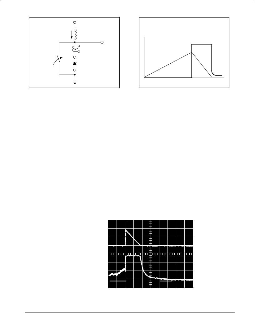
Figure 6. Test Circuit |
Figure 7. Current±Voltage Waveforms |
The unclamped inductive switching circuit shown in Figure 6 was used to demonstrate the controlled avalanche capability of the new ªE'' series Ultrafast rectifiers. A mercury switch was used instead of an electronic switch to simulate a noisy environment when the switch was being opened.
When S1 is closed at t0 the current in the inductor IL ramps up linearly; and energy is stored in the coil. At t1 the switch is opened and the voltage across the diode under test begins to rise rapidly, due to di/dt effects, when this induced voltage reaches the breakdown voltage of the diode, it is clamped at BVDUT and the diode begins to conduct the full load current which now starts to decay linearly through the diode, and goes to zero at t2.
By solving the loop equation at the point in time when S1 is opened; and calculating the energy that is transferred to the diode it can be shown that the total energy transferred is equal to the energy stored in the inductor plus a finite amount of energy from the VDD power supply while the diode is in breakdown (from t1 to t2) minus any losses due to finite com-
ponent resistances. Assuming the component resistive elements are small Equation (1) approximates the total energy transferred to the diode. It can be seen from this equation that if the VDD voltage is low compared to the breakdown voltage of the device, the amount of energy contributed by the supply during breakdown is small and the total energy can be assumed to be nearly equal to the energy stored in the coil during the time when S1 was closed, Equation (2).
The oscilloscope picture in Figure 8, shows the information obtained for the MUR8100E (similar die construction as the MUR1100E Series) in this test circuit conducting a peak current of one ampere at a breakdown voltage of 1300 volts, and using Equation (2) the energy absorbed by the MUR8100E is approximately 20 mjoules.
Although it is not recommended to design for this condition, the new ªE'' series provides added protection against those unforeseen transient viruses that can produce unexplained random failures in unfriendly environments.
EQUATION (1): |
|
|
||||
W |
1 LI |
2 |
|
BVDUT |
|
|
LPK BV |
±V |
|||||
AVAL [ 2 |
||||||
|
|
|
DUT DD |
|||
EQUATION (2): |
|
|
||||
|
1 |
2 |
|
|
|
|
WAVAL [ 2 LI LPK |
|
|
||||
CH1 |
500V |
A |
20ms |
953 V |
VERT |
CHANNEL 2: |
||
IL |
||||||||
CH2 |
50mV |
|
|
|
|
|||
|
|
|
|
|
|
|
0.5 AMPS/DIV. |
|
|
|
|
|
|
|
|
CHANNEL 1: |
|
|
|
|
|
|
|
|
VDUT |
|
|
|
|
|
|
|
|
500 VOLTS/DIV. |
|
|
|
|
|
|
|
|
TIME BASE: |
|
|
1 |
ACQUISITIONS |
|
|
217:33 HRS |
20 ms/DIV. |
||
|
|
|
|
|||||
|
SAVEREF SOURCE |
|
|
STACK |
|
|||
CH1 |
|
CH2 |
|
REF |
REF |
|
||
Figure 8. Current±Voltage Waveforms
4 |
Rectifier Device Data |
MUR190E MUR1100E
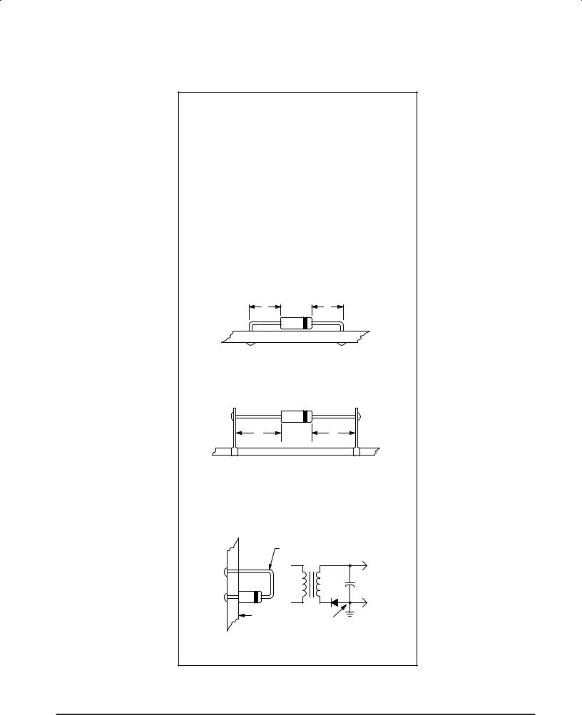
NOTE 1 Ð AMBIENT MOUNTING DATA
Data shown for thermal resistance junction to ambient (RθJA) for the mountings shown is to be used as typical guideline values for preliminary engineering or in case the tie point temperature cannot be measured.
TYPICAL VALUES FOR RqJA IN STILL AIR
Mounting |
Lead Length, L |
|
||||
|
Method |
1/8 |
1/4 |
1/2 |
Units |
|
1 |
|
|
52 |
65 |
72 |
°C/W |
2 |
|
RqJA |
67 |
80 |
87 |
°C/W |
3 |
|
|
|
50 |
|
°C/W |
MOUNTING METHOD 1
L |
L |
MOUNTING METHOD 2
L |
L |
Vector Pin Mounting
MOUNTING METHOD 3
L = 3/8″
 Board Ground Plane
P.C. Board with
1±1/2″ X 1±1/2″ Copper Surface
Rectifier Device Data |
5 |