Материал: 29010
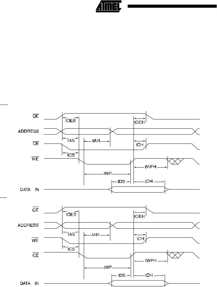
AC Byte Load Characteristics
Symbol |
Parameter |
Min |
Max |
Units |
||||||||
tAS, tOES |
Address, OE Set-up Time |
0 |
|
ns |
||||||||
|
|
|
|
|
|
|
|
|
|
|
|
|
tAH |
Address Hold Time |
50 |
|
ns |
||||||||
|
|
|
|
|
|
|
|
|
|
|
|
|
tCS |
Chip Select Set-up Time |
0 |
|
ns |
||||||||
tCH |
Chip Select Hold Time |
0 |
|
ns |
||||||||
|
|
|
|
|
|
|
|
|
|
|
|
|
|
|
|
|
|
|
|
|
|
|
|
||
tWP |
Write Pulse Width (WE or CE) |
90 |
|
ns |
||||||||
|
|
|
|
|
|
|
|
|
|
|
|
|
tDS |
Data Set-up Time |
35 |
|
ns |
||||||||
|
|
|
|
|
|
|
||||||
tDH, tOEH |
Data, OE Hold Time |
0 |
|
ns |
||||||||
tWPH |
Write Pulse Width High |
100 |
|
ns |
||||||||
|
|
|
|
|
|
|
|
|
|
|
|
|
AC Byte Load Waveforms
WE Controlled
CE Controlled
4-134 AT29C010A 
|
|
|
|
|
AT29C010A |
|
|
|
|
|
|
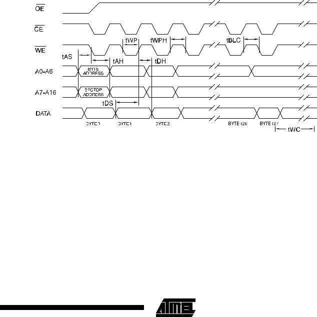
Program Cycle Characteristics |
|
|
|
|
|
|
|
|
|
|
|
Symbol |
Parameter |
Min |
Max |
Units |
|
tWC |
Write Cycle Time |
|
10 |
|
ms |
|
|
|
|
|
|
tAS |
Address Set-up Time |
0 |
|
|
ns |
tAH |
Address Hold Time |
50 |
|
|
ns |
tDS |
Data Set-up Time |
35 |
|
|
ns |
|
|
|
|
|
|
tDH |
Data Hold Time |
0 |
|
|
ns |
|
|
|
|
|
|
tWP |
Write Pulse Width |
90 |
|
|
ns |
tBLC |
Byte Load Cycle Time |
|
150 |
|
μs |
tWPH |
Write Pulse Width High |
100 |
|
|
ns |
|
|
|
|
|
|
Program Cycle Waveforms (1, 2, 3)
Notes: 1. |
A7 through A16 must specify the sector address |
3. All bytes that are not loaded within the sector being |
||
|
during each high to low transition of WE (or CE). |
programmed will be indeterminate. |
||
2. |
OE must be high when |
WE |
and CE are both low. |
|
4-135
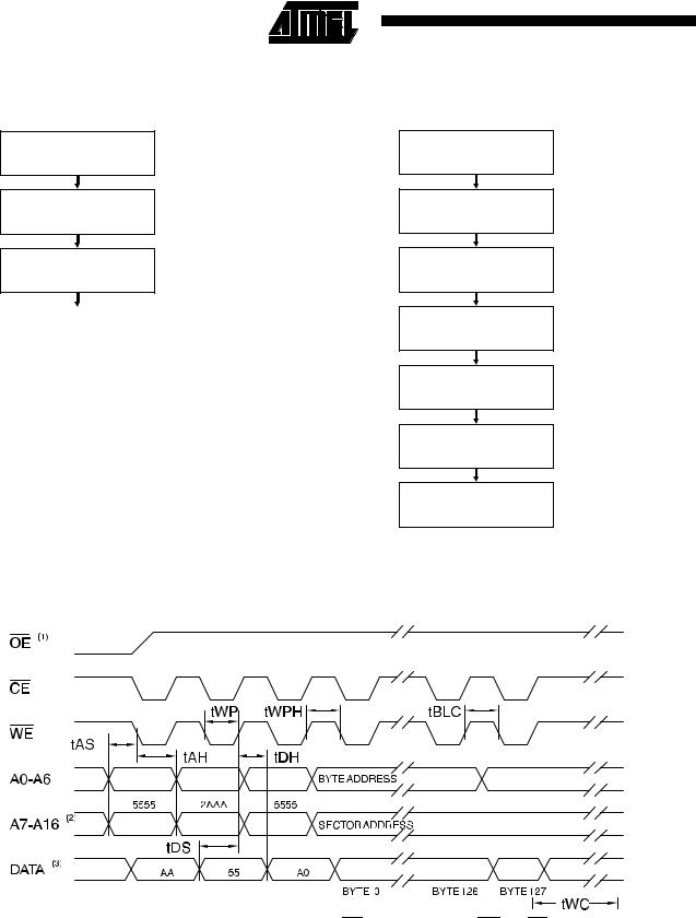
Software Data
Protection Enable Algorithm (1)
LOAD DATA AA |
|
TO |
|
ADDRESS 5555 |
|
LOAD DATA 55 |
|
TO |
|
ADDRESS 2AAA |
|
LOAD DATA A0 |
|
TO |
|
ADDRESS 5555 |
WRITES ENABLED |
|
LOAD DATA |
|
|
|
TO |
(4) |
ENTER DATA |
|
SECTOR (128 BYTES) |
|||
|
(2) |
||
|
|
PROTECT STATE |
Notes for software program code:
1.Data Format: I/O7 - I/O0 (Hex); Address Format: A14 - A0 (Hex).
2.Data Protect state will be activated at end of program cycle.
3.Data Protect state will be deactivated at end of program period.
4.128-bytes of data MUST BE loaded.
Software Data
Protection Disable Algorithm (1)
LOAD DATA AA |
|
|
TO |
|
|
ADDRESS 5555 |
|
|
LOAD DATA 55 |
|
|
TO |
|
|
ADDRESS 2AAA |
|
|
LOAD DATA 80 |
|
|
TO |
|
|
ADDRESS 5555 |
|
|
LOAD DATA AA |
|
|
TO |
|
|
ADDRESS 5555 |
|
|
LOAD DATA 55 |
|
|
TO |
|
|
ADDRESS 2AAA |
|
|
LOAD DATA 20 |
|
|
TO |
|
|
ADDRESS 5555 |
EXIT DATA |
|
|
(3) |
|
LOAD DATA |
PROTECT STATE |
|
|
||
TO |
(4) |
|
SECTOR (128 BYTES) |
||
|
Software Protected Program Cycle Waveform (1, 2, 3)
Notes: 1. A7 through A16 must specify the sector address |
2. |
OE must be high when WE and CE are both low. |
during each high to low transition of WE (or CE) |
3. |
All bytes that are not loaded within the sector being |
after the software code has been entered. |
|
programmed will be indeterminate. |
4-136 AT29C010A 
AT29C010A
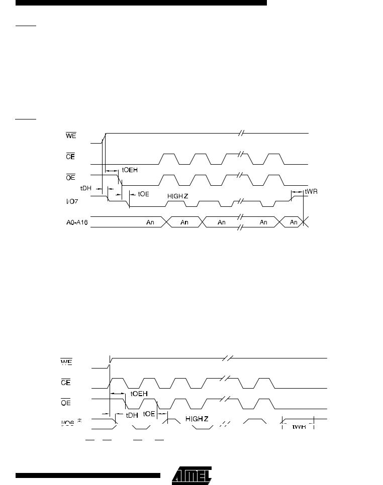
Data Polling Characteristics (1)
Symbol |
Parameter |
Min |
Typ |
Max |
Units |
||
tDH |
|
Data Hold Time |
10 |
|
|
ns |
|
|
|
|
|
|
|
|
|
|
|
|
|
|
|
|
|
tOEH |
|
OE Hold Time |
10 |
|
|
ns |
|
|
|
|
to Output Delay (2) |
|
|
|
|
tOE |
|
OE |
|
|
|
ns |
|
tWR |
|
Write Recovery Time |
0 |
|
|
ns |
|
|
|
|
|
|
|
|
|
Notes: 1. These parameters are characterized and not 100% tested. 2. See tOE spec in AC Read Characteristics.
Data Polling Waveforms
Toggle Bit Characteristics (1)
Symbol |
Parameter |
Min |
Typ |
Max |
Units |
||
|
|
|
|
|
|
|
|
tDH |
|
Data Hold Time |
10 |
|
|
ns |
|
|
|
|
|
|
|
|
|
|
|
|
|
|
|
|
|
tOEH |
|
OE Hold Time |
10 |
|
|
ns |
|
|
|
|
to Output Delay (2) |
|
|
|
|
tOE |
|
OE |
|
|
|
ns |
|
|
|
|
|
|
|
|
|
tOEHP |
|
OE High Pulse |
150 |
|
|
ns |
|
|
|
|
|
|
|
|
|
tWR |
|
Write Recovery Time |
0 |
|
|
ns |
|
|
|
|
|
|
|
|
|
Notes: 1. These parameters are characterized and not 100% tested. 2. See tOE spec in AC Read Characteristics.
Toggle Bit Waveforms (1, 2, 3)
Notes: 1. Toggling either OE or CE or both OE and CE will operate toggle bit.
2. Beginning and ending state of I/O6 will vary.
3.Any address location may be used but the address should not vary.
4-137
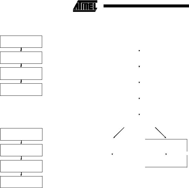
Software Product
Identification Entry (1)
LOAD DATA AA
TO
ADDRESS 5555
LOAD DATA 55
TO
ADDRESS 2AAA
LOAD DATA 90
TO
ADDRESS 5555
PAUSE 10 mS
ENTER PRODUCT
IDENTIFICATION
MODE (2, 3, 5)
Software Product
Identification Exit (1)
LOAD DATA AA
TO
ADDRESS 5555
LOAD DATA 55
TO
ADDRESS 2AAA
LOAD DATA F0
TO
ADDRESS 5555
PAUSE 10 mS
EXIT PRODUCT
IDENTIFICATION
MODE (4)
Notes for software product identification:
1.Data Format: I/O7 - I/O0 (Hex); Address Format: A14 - A0 (Hex).
2.A1 - A16 = VIL.
Manufacture Code is read for A0 = VIL; Device Code is read for A0 = VIH.
3.The device does not remain in identification mode if powered down.
4.The device returns to standard operation mode.
5.Manufacturer Code: 1F Device Code: D5
Boot Block Lockout
Feature Enable Algorithm (1)
|
|
|
LOAD DATA AA |
|
|
|||
|
|
|
|
TO |
|
|
||
|
|
|
ADDRESS 5555 |
|
|
|||
|
|
|
|
|
|
|
|
|
|
|
|
|
|
|
|
|
|
|
|
|
LOAD DATA 55 |
|
|
|||
|
|
|
|
TO |
|
|
||
|
|
|
ADDRESS 2AAA |
|
|
|||
|
|
|
|
|
|
|
|
|
|
|
|
|
|
|
|
|
|
|
|
|
LOAD DATA 80 |
|
|
|||
|
|
|
|
TO |
|
|
||
|
|
|
ADDRESS 5555 |
|
|
|||
|
|
|
|
|
|
|
|
|
|
|
|
|
|
|
|
|
|
|
|
|
LOAD DATA AA |
|
|
|||
|
|
|
|
TO |
|
|
||
|
|
|
ADDRESS 5555 |
|
|
|||
|
|
|
|
|
|
|
|
|
|
|
|
|
|
|
|
|
|
|
|
|
LOAD DATA 55 |
|
|
|||
|
|
|
|
TO |
|
|
||
|
|
|
ADDRESS 2AAA |
|
|
|||
|
|
|
|
|
|
|
|
|
|
|
|
|
|||||
|
|
|
LOAD DATA 40 |
|
||||
|
|
|
|
TO |
|
|||
|
|
|
ADDRESS 5555 |
|
||||
|
|
|
|
|
|
|
|
|
LOAD DATA 00 |
|
|
|
LOAD DATA FF |
||||
TO |
|
|
|
|
TO |
|||
ADDRESS 00000 (2) |
|
|
|
ADDRESS FFFFF (3) |
||||
|
|
|
|
|
|
|
|
|
|
|
|
|
|
|
|||
PAUSE 10 mS |
|
|
|
PAUSE 10 mS |
||||
|
|
|
|
|
|
|
|
|
Notes for boot block lockout feature enable:
1.Data Format: I/O7 - I/O0 (Hex); Address Format: A14 - A0 (Hex).
2.Lockout feature set on lower address boot block.
3.Lockout feature set on higher address boot block.
4-138 AT29C010A 