Материал: 9015
Philips Semiconductors Product specification
PowerMOS transistor |
|
|
|
|
|
BUK102-50GL |
|
|||||||
Logic level TOPFET |
|
|
|
|
|
|
|
|
|
|
|
|
|
|
|
|
|
|
|
|
|
|
|
|
|
|
|||
DESCRIPTION |
|
QUICK REFERENCE DATA |
|
|
|
|
|
|
|
|
|
|||
|
|
|
|
|
|
|
|
|
|
|
|
|||
Monolithic temperature and |
|
SYMBOL |
|
PARAMETER |
|
|
|
MAX. |
|
UNIT |
|
|||
overload protected logic level power |
|
|
|
|
|
|
|
|
|
|
|
|
|
|
|
|
|
|
|
|
|
|
|
|
|
|
|
|
|
MOSFET in a 3 pin plastic |
|
VDS |
|
Continuous drain source voltage |
|
50 |
|
|
V |
|
||||
envelope, intended as a general |
|
ID |
|
Continuous drain current |
|
45 |
|
|
A |
|
||||
purpose switch for automotive |
|
PD |
|
Total power dissipation |
|
125 |
|
|
W |
|
||||
systems and other applications. |
|
Tj |
|
Continuous junction temperature |
|
150 |
|
|
˚C |
|
||||
APPLICATIONS |
|
RDS(ON) |
|
Drain-source on-state resistance |
|
35 |
|
|
mΩ |
|
||||
|
|
|
|
VIS = 5 V |
|
|
|
|
|
|
|
|
|
|
General controller for driving |
|
|
|
|
|
|
|
|
|
|
|
|
|
|
lamps |
|
|
|
|
|
|
|
|
|
|
|
|
|
|
motors |
|
|
|
|
|
|
|
|
|
|
|
|
|
|
solenoids |
|
|
|
|
|
|
|
|
|
|
|
|
|
|
heaters |
|
|
|
|
|
|
|
|
|
|
|
|
|
|
FEATURES |
|
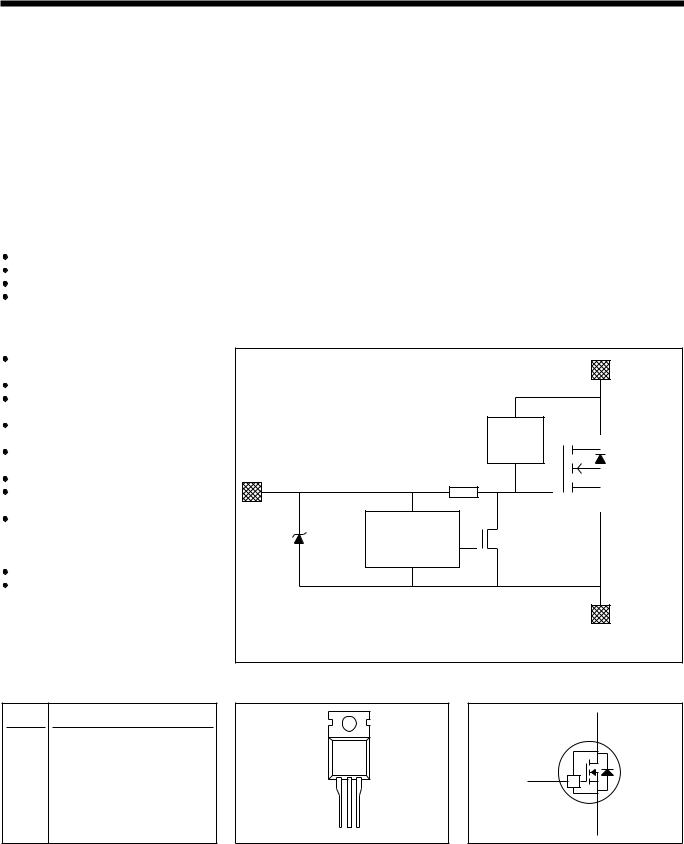
FUNCTIONAL BLOCK DIAGRAM |
|
|
|
|
|
|
|
|
|
|||
Vertical power DMOS output |
|
|
|
|
stage |
|
|
DRAIN |
|
Low on-state resistance |
|
|
|
|
Overload protection against |
|
|
|
|
over temperature |
|
|
|
|
Overload protection against |
|
O/V |
|
|
short circuit load |
|
|
||
|
CLAMP |
|
||
Latched overload protection |
|
POWER |
||
reset by input |
INPUT |
|
||
|
MOSFET |
|||
5 V input level |
|
RIG |
||
Low threshold voltage |
|
|
|
|
also allows 5 V control |
|
|
|
|
Control of power MOSFET |
LOGIC AND |
|
|
|
and supply of overload |
|
|
||
PROTECTION |
|
|
||
protection circuits |
|
|
||
derived from input |
|
|
|
|
ESD protection on input pin |
|
|
|
|
Overvoltage clamping for turn |
|
|
|
|
off of inductive loads |
|
|
SOURCE |
|
|
|
|
|
|
|
|
Fig.1. Elements of the TOPFET. |
|
|
PINNING - TO220AB |
PIN CONFIGURATION |
SYMBOL |
|
|
PIN |
DESCRIPTION |
tab |
|
D |
|
|
TOPFET |
||
1 |
input |
|
|
|
|
|
|
||
2 |
drain |
|
I |
|
|
|
|
|
|
|
|
|
P |
|
3 |
source |
|
|
|
tab |
drain |
1 2 3 |
|
S |
|
|
|
||
January 1993 |
1 |
Rev 1.200 |

Philips Semiconductors Product specification
PowerMOS transistor |
|
|
|
|
BUK102-50GL |
|
||
Logic level TOPFET |
|
|
|
|
|
|
|
|
|
|
|
|
|
|
|
|
|
LIMITING VALUES |
|
|
|
|
|
|
|
|
Limiting values in accordance with the Absolute Maximum Rating System (IEC 134) |
|
|
|
|
||||
|
|
|
|
|
|
|
||
SYMBOL |
PARAMETER |
CONDITIONS |
|
MIN. |
MAX. |
UNIT |
|
|
|
|
|
|
|
|
|
|
|
VDSS |
Continuous off-state drain source |
VIS = 0 V |
|
- |
50 |
V |
|
|
|
voltage1 |
|
|
|
|
|
|
|
VIS |
Continuous input voltage |
- |
≤ 25 ˚C; VIS = 5 V |
|
0 |
6 |
V |
|
ID |
Continuous drain current |
Tmb |
|
- |
45 |
A |
|
|
ID |
Continuous drain current |
Tmb |
≤ 100 ˚C; VIS = 5 V |
|
- |
28 |
A |
|
IDRM |
Repetitive peak on-state drain current |
Tmb |
≤ 25 ˚C; VIS = 5 V |
|
- |
180 |
A |
|
PD |
Total power dissipation |
Tmb |
≤ 25 ˚C |
|
- |
125 |
W |
|
Tstg |
Storage temperature |
- |
|
|
-55 |
150 |
˚C |
|
T |
Continuous junction temperature2 |
normal operation |
|
- |
150 |
˚C |
|
|
j |
|
|
|
|
|
|
|
|
Tsold |
Lead temperature |
during soldering |
|
- |
250 |
˚C |
|
|
OVERLOAD PROTECTION LIMITING VALUES
With the protection supply provided via the input pin, TOPFET can protect itself from two types of overload.
SYMBOL |
PARAMETER |
CONDITIONS |
MIN. |
MAX. |
UNIT |
|
|
|
|
|
|
|
|
V |
Protection supply voltage3 |
for valid protection |
4 |
- |
V |
|
ISP |
|
|
|
|
|
|
|
Over temperature protection |
|
|
|
|
|
VDDP(T) |
Protected drain source supply voltage |
VIS = 5 |
V |
- |
50 |
V |
|
Short circuit load protection |
|
|
|
|
|
V |
Protected drain source supply voltage4 |
V = 5 |
V |
- |
24 |
V |
DDP(P) |
|
IS |
|
|
|
|
PDSM |
Instantaneous overload dissipation |
Tmb = 25 ˚C |
- |
2.1 |
kW |
|
OVERVOLTAGE CLAMPING LIMITING VALUES
At a drain source voltage above 50 V the power MOSFET is actively turned on to clamp overvoltage transients.
SYMBOL |
PARAMETER |
CONDITIONS |
MIN. |
MAX. |
UNIT |
|
|
|
|
|
|
|
|
IDROM |
Repetitive peak clamping current |
VIS = 0 V |
- |
45 |
A |
|
EDSM |
Non-repetitive clamping energy |
Tmb |
≤ 25 ˚C; IDM = 25 A; |
- |
1 |
J |
|
|
VDD |
≤ 25 V; inductive load |
|
|
|
EDRM |
Repetitive clamping energy |
Tmb |
≤ 85 ˚C; IDM = 16 A; |
- |
80 |
mJ |
|
|
VDD |
≤ 20 V; f = 250 Hz |
|
|
|
ESD LIMITING VALUE
SYMBOL |
PARAMETER |
CONDITIONS |
MIN. |
MAX. |
UNIT |
|
|
|
|
|
|
VC |
Electrostatic discharge capacitor |
Human body model; |
- |
2 |
kV |
|
voltage |
C = 250 pF; R = 1.5 kΩ |
|
|
|
|
|
|
|
|
|
1 Prior to the onset of overvoltage clamping. For voltages above this value, safe operation is limited by the overvoltage clamping energy.
2 A higher Tj is allowed as an overload condition but at the threshold Tj(TO) the over temperature trip operates to protect the switch.
3 The input voltage for which the overload protection circuits are functional.
4 The device is able to self-protect against a short circuit load providing the drain-source supply voltage does not exceed VDDP(P) maximum. For further information, refer to OVERLOAD PROTECTION CHARACTERISTICS.
January 1993 |
2 |
Rev 1.200 |

Philips Semiconductors Product specification
PowerMOS transistor |
|
|
BUK102-50GL |
|
|||
Logic level TOPFET |
|
|
|
|
|
|
|
|
|
|
|
|
|
|
|
THERMAL CHARACTERISTICS |
|
|
|
|
|
|
|
|
|
|
|
|
|
|
|
SYMBOL |
PARAMETER |
CONDITIONS |
MIN. |
TYP. |
MAX. |
UNIT |
|
|
|
|
|
|
|
|
|
|
Thermal resistance |
|
|
|
|
|
|
Rth j-mb |
Junction to mounting base |
- |
- |
0.8 |
1.0 |
K/W |
|
Rth j-a |
Junction to ambient |
in free air |
- |
60 |
- |
K/W |
|
STATIC CHARACTERISTICS |
|
|
|
|
|
|
|
Tmb = 25 ˚C unless otherwise specified |
|
|
|
|
|
|
|
|
|
|
|
|
|
|
|
SYMBOL |
PARAMETER |
CONDITIONS |
MIN. |
TYP. |
MAX. |
UNIT |
|
|
|
|
|
|
|
|
|
V(CL)DSS |
Drain-source clamping voltage |
VIS = 0 V; ID = 10 mA |
50 |
- |
- |
V |
|
V(CL)DSS |
Drain-source clamping voltage |
VIS = 0 V; IDM = 2 A; tp £ 300 ms; |
- |
- |
70 |
V |
|
|
|
d £ 0.01 |
|
|
|
mA |
|
IDSS |
Zero input voltage drain current |
VDS = 12 V; VIS = 0 V |
- |
0.5 |
10 |
|
|
IDSS |
Zero input voltage drain current |
VDS = 50 V; VIS = 0 V |
- |
1 |
20 |
mA |
|
IDSS |
Zero input voltage drain current |
VDS = 40 V; VIS = 0 V; Tj = 125 ˚C |
- |
10 |
100 |
mA |
|
RDS(ON) |
Drain-source on-state |
IDM = 25 A; VIS = 5 V |
- |
30 |
35 |
mW |
|
|
resistance |
tp £ 300 ms; d £ 0.01 |
|
|
|
|
|
OVERLOAD PROTECTION CHARACTERISTICS
TOPFET switches off when one of the overload thresholds is reached. It remains latched off until reset by the input.
SYMBOL |
PARAMETER |
CONDITIONS |
MIN. |
TYP. |
MAX. |
UNIT |
|
|
|
|
|
|
|
EDS(TO) |
Short circuit load protection1 |
Tmb = 25 ˚C; L £ 10 mH |
|
|
|
|
Overload threshold energy |
VDD = 13 V; VIS = 5 V |
- |
1.1 |
- |
J |
|
td sc |
Response time |
VDD = 13 V; VIS = 5 V |
- |
0.8 |
- |
ms |
|
Over temperature protection |
VIS = 5 V; from ID ³ 2 A2 |
|
|
|
|
Tj(TO) |
Threshold junction temperature |
150 |
- |
- |
˚C |
INPUT CHARACTERISTICS
Tmb = 25 ˚C unless otherwise specified. The supply for the logic and overload protection is taken from the input.
SYMBOL |
PARAMETER |
CONDITIONS |
MIN. |
TYP. |
MAX. |
UNIT |
|
|
|
|
|
|
|
VIS(TO) |
Input threshold voltage |
VDS = 5 V; ID = 1 mA |
1.0 |
1.5 |
2.0 |
V |
IIS |
Input supply current |
VIS = 5 V; normal operation |
- |
0.2 |
0.35 |
mA |
V |
Protection reset voltage3 |
|
2.0 |
2.6 |
3.5 |
V |
ISR |
|
|
|
|
|
|
VISR |
Protection reset voltage |
Tj = 150 ˚C |
1.0 |
- |
- |
|
IISL |
Input supply current |
VIS = 5 V; protection latched |
2 |
3.8 |
10 |
mA |
V(BR)IS |
Input clamp voltage |
II = 10 mA |
6 |
- |
- |
V |
RIG |
Input series resistance |
to gate of power MOSFET |
- |
1.5 |
- |
kW |
1 The short circuit load protection is able to save the device providing the instantaneous on-state dissipation is less than the limiting value for
PDSM, which is always the case when VDS is less than VDSP maximum. Refer to OVERLOAD PROTECTION LIMITING VALUES.
2 The over temperature protection feature requires a minimum on-state drain source voltage for correct operation. The specified minimum ID ensures this condition.
3 The input voltage below which the overload protection circuits will be reset.
January 1993 |
3 |
Rev 1.200 |

Philips Semiconductors Product specification
PowerMOS transistor |
|
|
|
|
|
BUK102-50GL |
|
|||||
Logic level TOPFET |
|
|
|
|
|
|
|
|
|
|
|
|
|
|
|
|
|
|
|
|
|
|
|
|
|
TRANSFER CHARACTERISTICS |
|
|
|
|
|
|
|
|
|
|
|
|
Tmb = 25 ˚C |
|
|
|
|
|
|
|
|
|
|
|
|
SYMBOL |
PARAMETER |
CONDITIONS |
MIN. |
TYP. |
|
MAX. |
UNIT |
|
||||
gfs |
Forward transconductance |
VDS = 10 V; IDM = 25 A tp ≤ 300 μs; |
17 |
28 |
|
- |
|
S |
|
|||
|
|
δ ≤ |
0.01 |
|
|
|
|
|
|
|
|
|
I |
Drain current1 |
V |
= 13 V; V = 5 V |
- |
60 |
|
- |
|
A |
|
||
D(SC) |
|
DS |
|
IS |
|
|
|
|
|
|
|
|
SWITCHING CHARACTERISTICS |
|
|
|
|
|
|
|
|
|
|
|
|
Tmb = 25 ˚C. RI = 50 Ω . Refer to waveform figures and test circuits. |
|
|
|
|
|
|
|
|
||||
|
|
|
|
|
|
|
|
|
||||
SYMBOL |
PARAMETER |
CONDITIONS |
MIN. |
TYP. |
|
MAX. |
UNIT |
|
||||
|
|
|
|
|
|
|
|
|
|
|||
td on |
Turn-on delay time |
VDD = 13 V; VIS = 5 V |
- |
2 |
|
- |
|
μs |
|
|||
tr |
Rise time |
resistive load RL = 1.1 Ω |
- |
8 |
|
- |
|
μs |
|
|||
td off |
Turn-off delay time |
VDD = 13 V; VIS = 0 V |
- |
8 |
|
- |
|
μs |
|
|||
tf |
Fall time |
resistive load RL = 1.1 Ω |
- |
8 |
|
- |
|
μs |
|
|||
td on |
Turn-on delay time |
VDD = 13 V; VIS = 5 V |
- |
3.7 |
|
- |
|
μs |
|
|||
tr |
Rise time |
inductive load IDM = 11 A |
- |
3.7 |
|
- |
|
μs |
|
|||
td off |
Turn-off delay time |
VDD = 13 V; VIS = 0 V |
- |
13 |
|
- |
|
μs |
|
|||
tf |
Fall time |
inductive load IDM = 11 A |
- |
1.4 |
|
- |
|
μs |
|
|||
REVERSE DIODE LIMITING VALUE |
|
|
|
|
|
|
|
|
|
|
|
|
|
|
|
|
|
|
|
|
|
|
|
||
SYMBOL |
PARAMETER |
|
|
CONDITIONS |
MIN. |
|
MAX. |
|
UNIT |
|
||
|
|
|
|
|
|
|
|
|
|
|
|
|
IS |
Continuous forward current |
|
|
Tmb ≤ 25 ˚C; VIS = 0 V |
- |
|
|
50 |
|
A |
|
|
|
|
|
|
|
|
|
|
|
|
|
|
|
REVERSE DIODE CHARACTERISTICS |
|
|
|
|
|
|
|
|
|
|
||
Tmb = 25 ˚C |
|
|
|
|
|
|
|
|
|
|
|
|
|
|
|
|
|
|
|
|
|
|
|
|
|
SYMBOL |
PARAMETER |
CONDITIONS |
MIN. |
TYP. |
|
MAX. |
UNIT |
|
||||
|
|
|
|
|
|
|
|
|
|
|
|
|
VSDS |
Forward voltage |
IS = 50 A; VIS = 0 V; tp = 300 μs |
- |
1.0 |
|
1.5 |
V |
|
||||
t |
Reverse recovery time |
not applicable2 |
- |
- |
|
- |
|
- |
|
|||
rr |
|
|
|
|
|
|
|
|
|
|
|
|
ENVELOPE CHARACTERISTICS |
|
|
|
|
|
|
|
|
|
|
|
|
|
|
|
|
|
|
|
|
|
|
|
|
|
SYMBOL |
PARAMETER |
CONDITIONS |
MIN. |
TYP. |
|
MAX. |
UNIT |
|
||||
|
|
|
|
|
|
|
|
|
|
|
|
|
Ld |
Internal drain inductance |
Measured from contact screw on |
- |
3.5 |
|
- |
|
nH |
|
|||
|
|
tab to centre of die |
|
|
|
|
|
|
|
|
||
Ld |
Internal drain inductance |
Measured from drain lead 6 mm |
- |
4.5 |
|
- |
|
nH |
|
|||
|
|
from package to centre of die |
|
|
|
|
|
|
|
|
||
Ls |
Internal source inductance |
Measured from source lead 6 mm |
- |
7.5 |
|
- |
|
nH |
|
|||
|
|
from package to source bond pad |
|
|
|
|
|
|
|
|
||
|
|
|
|
|
|
|
|
|
|
|
|
|
1 During overload before short circuit load protection operates.
2 The reverse diode of this type is not intended for applications requiring fast reverse recovery.
January 1993 |
4 |
Rev 1.200 |
Philips Semiconductors |
Product specification |
|
|
PowerMOS transistor |
|
|
|
|
|
|
|
|
|
BUK102-50GL |
|||||||||||
Logic level TOPFET |
|
|
|
|
|
|
|
|
|
|
|
|
|
|
|
||||||
|
120 |
PD% |
|
|
Normalised Power Derating |
Zth / (K/W) |
|
|
|
|
|
BUK102-50GL |
|||||||||
|
|
|
|
|
|
|
|
|
10 |
|
|
|
|
|
|
|
|
|
|
|
|
|
110 |
|
|
|
|
|
|
|
|
|
|
|
|
|
|
|
|
|
|
|
|
|
100 |
|
|
|
|
|
|
|
|
|
|
|
|
|
|
|
|
|
|
|
|
|
90 |
|
|
|
|
|
|
|
|
1 |
D = |
|
|
|
|
|
|
|
|
|
|
|
80 |
|
|
|
|
|
|
|
|
|
0.5 |
|
|
|
|
|
|
|
|
|
|
|
70 |
|
|
|
|
|
|
|
|
|
0.2 |
|
|
|
|
|
|
|
|
|
|
|
60 |
|
|
|
|
|
|
|
|
0.1 |
0.1 |
|
|
|
|
|
|
|
|
|
|
|
50 |
|
|
|
|
|
|
|
|
|
0.05 |
|
|
|
|
|
|
|
|
|
|
|
40 |
|
|
|
|
|
|
|
|
|
0.02 |
|
|
|
|
|
|
|
|
|
|
|
|
|
|
|
|
|
|
|
|
|
|
|
|
|
|
|
|
|
|
|
|
|
30 |
|
|
|
|
|
|
|
|
0.01 |
0 |
|
|
|
P |
|
tp |
D = |
tp |
|
|
|
20 |
|
|
|
|
|
|
|
|
|
|
|
D |
|
|
T |
|
||||
|
|
|
|
|
|
|
|
|
|
|
|
|
|
|
|
|
|
|
|
|
|
|
10 |
|
|
|
|
|
|
|
|
|
|
|
|
|
|
|
|
T |
|
t |
|
|
|
|
|
|
|
|
|
|
|
|
|
|
|
|
|
|
|
|
|
||
|
0 |
|
|
|
|
|
|
|
|
0.001 |
|
|
|
|
|
|
|
|
|
|
|
|
0 |
20 |
40 |
60 |
80 |
100 |
120 |
140 |
|
|
|
|
|
|
|
|
|
|
|
||
|
|
1E-07 |
|
1E-05 |
|
1E-03 |
|
|
1E-01 |
|
|
1E+01 |
|||||||||
|
|
|
|
|
|
Tmb / |
C |
|
|
|
|
|
|
|
t / s |
|
|
|
|
|
|
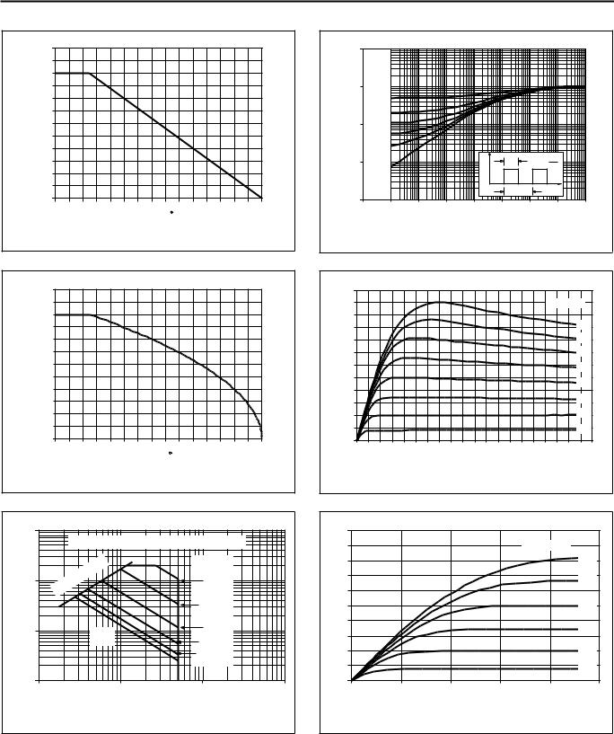
Fig.2. |
Normalised limiting power dissipation. |
Fig.5. |
Transient thermal impedance. |
|
|||||||||||||||||
|
|
|
PD% = 100×PD/PD(25 ˚C) = f(Tmb) |
|
Zth j-mb = f(t); parameter D = tp/T |
|
|
||||||||||||||
|
120 |
ID% |
|
|
Normalised Current Derating |
ID / A |
|
|
|
|
|
|
BUK102-50GL |
||||||||
|
|
|
|
|
|
|
|
|
120 |
|
|
|
|
|
|
|
|
|
|
|
|
|
110 |
|
|
|
|
|
|
|
|
110 |
|
|
|
|
|
|
|
|
VIS / V = |
||
|
100 |
|
|
|
|
|
|
|
|
100 |
|
|
|
|
|
|
|
|
|
|
|
|
90 |
|
|
|
|
|
|
|
|
90 |
|
|
|
|
|
|
|
|
|
|
6.0 |
|
80 |
|
|
|
|
|
|
|
|
80 |
|
|
|
|
|
|
|
|
|
|
5.5 |
|
70 |
|
|
|
|
|
|
|
|
70 |
|
|
|
|
|
|
|
|
|
|
5.0 |
|
60 |
|
|
|
|
|
|
|
|
60 |
|
|
|
|
|
|
|
|
|
|
4.5 |
|
|
|
|
|
|
|
|
|
|
|
|
|
|
|
|
|
|
|
|
|
|
|
50 |
|
|
|
|
|
|
|
|
50 |
|
|
|
|
|
|
|
|
|
|
4.0 |
|
40 |
|
|
|
|
|
|
|
|
40 |
|
|
|
|
|
|
|
|
|
|
|
|
|
|
|
|
|
|
|
|
|
|
|
|
|
|
|
|
|
|
3.5 |
||
|
30 |
|
|
|
|
|
|
|
|
30 |
|
|
|
|
|
|
|
|
|
|
|
|
|
|
|
|
|
|
|
|
|
|
|
|
|
|
|
|
|
|
|
||
|
20 |
|
|
|
|
|
|
|
|
20 |
|
|
|
|
|
|
|
|
|
|
3.0 |
|
10 |
|
|
|
|
|
|
|
|
10 |
|
|
|
|
|
|
|
|
|
|
2.5 |
|
0 |
0 |
20 |
40 |
60 |
80 |
100 |
120 |
140 |
0 |
|
|
|
|
|
|
|
|
|
|
|
|
|
0 |
2 |
4 |
6 |
8 |
10 |
12 |
|
14 |
16 |
18 |
20 |
||||||||
|
|
|
|
|
|
Tmb / |
C |
|
|
|
|
|
|
|
VDS / V |
|
|
|
|
|
|
|
Fig.3. |
Normalised continuous drain current. |
Fig.6. |
Typical output characteristics, Tj |
= 25 ˚C. |
||||||||||||||||
ID% = 100×ID/ID(25 ˚C) = f(Tmb); conditions: VIS = 5 V |
ID = f(VDS); parameter VIS; tp = 250 ms |
& tp < td sc |
|||||||||||||||||||
1000 |
ID & IDM / A |
|
|
|
|
|
BUK102-50GL |
ID / A |
|
|
|
|
|
|
|
BUK102-50GL |
|||||
|
|
|
|
|
|
|
|
|
100 |
|
|
|
|
|
|
|
|
|
|
|
|
|
|
|
Overload protection characteristics not shown |
|
90 |
|
|
|
|
|
|
|
VIS / V = |
|
|||||||
|
|
|
|
|
|
|
|
|
|
|
|
|
|
|
|
|
|
||||
|
|
|
|
|
|
|
tp = |
|
80 |
|
|
|
|
|
|
|
|
|
|
5.0 |
|
|
|
|
VDS/ID |
|
|
|
70 |
|
|
|
|
|
|
|
|
|
|
|
|||
|
|
|
|
|
|
|
|
|
|
|
|
|
|
|
|
|
|
|
|||
100 |
|
|
= |
|
|
|
|
10 us |
|
|
|
|
|
|
|
|
|
|
|
4.5 |
|
|
RDS(ON) |
|
|
|
|
|
|
|
|
|
|
|
|
|
|
|
|
||||
|
|
|
|
|
|
|
|
|
|
|
|
|
|
|
|
|
|
|
|||
|
|
|
|
|
|
|
|
|
|
60 |
|
|
|
|
|
|
|
|
|
|
|
|
|
|
|
|
|
|
|
100 us |
|
50 |
|
|
|
|
|
|
|
|
|
|
4.0 |
|
|
|
|
|
|
|
|
1 ms |
|
40 |
|
|
|
|
|
|
|
|
|
|
3.5 |
10 |
|
|
|
DC |
|
|
|
|
30 |
|
|
|
|
|
|
|
|
|
|
||
|
|
|
|
|
|
|
|
|
|
|
|
|
|
|
|
|
|
|
|||
|
|
|
|
|
|
|
10 ms |
|
|
|
|
|
|
|
|
|
|
|
|
||
|
|
|
|
|
|
|
|
|
20 |
|
|
|
|
|
|
|
|
|
|
3.0 |
|
|
|
|
|
|
|
|
100 ms |
|
|
|
|
|
|
|
|
|
|
|
|||
|
|
|
|
|
|
|
|
|
|
|
|
|
|
|
|
|
|
|
|
||
|
|
|
|
|
|
|
|
|
|
10 |
|
|
|
|
|
|
|
|
|
|
2.5 |
|
|
|
|
|
|
|
|
|
|
|
|
|
|
|
|
|
|
|
|
|
|
1 |
|
|
|
|
|
|
|
|
|
0 |
|
1 |
|
|
|
3 |
|
|
|
|
5 |
|
1 |
|
|
|
10 |
|
100 |
|
0 |
|
|
2 |
|
|
|
4 |
|||||
|
|
|
|
|
|
VDS / V |
|
|
|
|
|
|
|
VDS / V |
|
|
|
|
|
|
|
Fig.4. Safe operating area. Tmb = 25 ˚C |
Fig.7. Typical on-state characteristics, Tj = 25 ˚C. |
ID & IDM = f(VDS); IDM single pulse; parameter tp |
ID = f(VDS); parameter VIS; tp = 250 ms |
January 1993 |
5 |
Rev 1.200 |