Материал: 9100
Philips Semiconductors |
Product specification |
|
|
Insulated Gate Bipolar Transistor |
BUK856-400 IZ |
Protected Logic-Level IGBT |
|
|
|
dVce/dt (V/us) |
|
|
|
PMG35A |
|
150 |
|
|
|
|
|
100 |
|
|
|
|
|
50 |
|
|
|
|
|
0 |
|
|
|
|
|
0 |
1 |
2 |
3 |
4 |
5 |
|
|
Rg / kOhm |
|
|
|
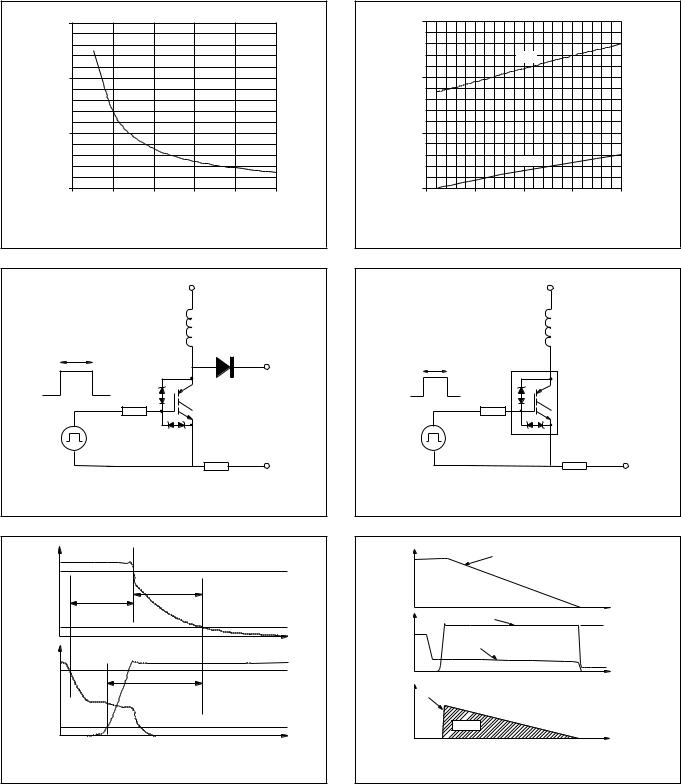
Fig.19. Typical Turn-off dVCE/dt vs. RG conditions: Tj=125 ˚C; IC=8 A; VCL=300 V; LC=5 mH.
Vcc
Lc
t p : adjust for correct Ic
VCL
D.U.T.
R G
VGE
IC measure
0V
0R1
Fig.20. Test circuit for inductive load switching times.
V(BR)ECS / V |
|
BUK856-400IZ |
||
35 |
|
|
|
|
|
|
typ. |
|
|
30 |
|
|
|
|
25 |
|
|
|
|
|
|
min. |
|
|
20 |
0 |
50 |
100 |
150 |
-50 |
||||
|
|
Tj / degC |
|
|
Fig.22. Reverse Breakdown Voltage
V(BR)ECS = f(Tj); conditions: IEC = 50 mA
Vcc
Lc
t p : adjust for correct Ic
D.U.T.
RG
VGE
IC measure
0V
0R1
Fig.23. Test circuit for clamped turn-off energy test
I C |
90% |
tf |
td(off) |
10% |
t |
VCE |
VGE |
90% |
tc |
10% |
t |
Fig.21. Definitions of inductive load switching times.
I
Ic |
V |
t |
Vce |
|
|
V(cl)cer |
|
Vge |
|
t |
P |
|
Vce x Ic
Ecer
t
Fig.24. Definition of clamping energy ECER
August 1994 |
6 |
Rev. 1.100 |
Philips Semiconductors Product specification
Insulated Gate Bipolar Transistor |
BUK856-400 IZ |
|
Protected Logic-Level IGBT |
|
|
MECHANICAL DATA |
|
|
Dimensions in mm |
4,5 |
|
Net Mass: 2 g |
||
max |
||
10,3 |
|
|
max |
1,3 |
|
3,7 |
||
|
||
2,8 |
5,9 |
|
|
min |
|
|
15,8 |
|
|
max |
3,0 max |
3,0 |
|
not tinned |
||
|
|
|
13,5 |
|
|
|
min |
|
1,3 |
|
|
|
max |
1 2 3 |
|
|
(2x) |
|
0,9 max (3x) |
0,6 |
|
|
|
|
|
2,54 2,54 |
|
2,4 |
|
|
|
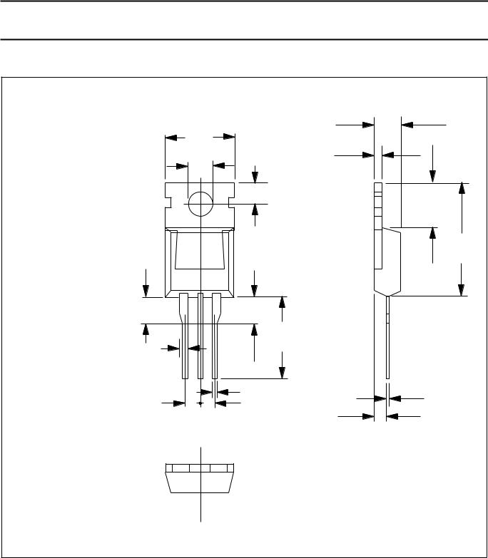
Fig.25. TO220AB; pin 2 connected to mounting base.
Notes
1.Observe the general handling precautions for electrostatic-discharge sensitive devices (ESDs) to prevent damage to MOS gate oxide.
2.Accessories supplied on request: refer to mounting instructions for TO220 envelopes.
3.Epoxy meets UL94 V0 at 1/8".
August 1994 |
7 |
Rev. 1.100 |