Материал: 9487

DISCRETE SEMICONDUCTORS
OM2063
Wideband amplifier module
Product specification |
1995 Nov 28 |
Supersedes data of June 1991
File under Discrete Semiconductors, SC16
Philips Semiconductors |
Product specification |
|
|
Wideband amplifier module |
OM2063 |
|
|
|
|
DESCRIPTION
A three-stage wideband amplifier in hybrid integrated circuit form on a thin-film substrate. The device is intended for use in mast-head booster amplifiers, as an amplifier in MATV systems and as a general purpose amplifier for VHF and UHF applications.
PINNING |
|
|
|
|
|
|
|
|
|
|
|
|
|
|
|
|
|
|
|
|
|
|
|
|
|
|
|
|
|
|
|
|
|
|
|
PIN |
DESCRIPTION |
|
|
|
|
|
|
|
|
|
|
|
|
|
|
|
|
|
|
|
|
|
|
|
|
|
|
|
|
|
|
|
|
|
|
1 |
input |
|
|
|
|
|
|
|
pin 1 identification |
|
|
|
|||||
|
|
|
|
handbook, halfpage |
|
|
|
|
|||||||||
2 |
common |
|
|
|
|
|
|
|
|
|
|
|
|
||||
|
|
|
|
|
|
|
|
|
|
|
|
|
|
|
|
||
3 |
common |
|
|
|
|
|
|
|
1 |
|
|
|
|
|
|
|
|
|
|
|
|
|
|
|
|
|
|
|
|
|
|
|
|||
4 |
supply (+) |
|
|
|
|
|
|
|
|
|
|
|
|
|
|
|
|
|
|
|
|
|
|
|
|
|
|
|
|
|
|
|
|
||
|
|
|
|
|
|
|
|
|
|
|
|
|
|
|
|
||
5 |
common |
|
|
8 |
7 6 5 4 |
3 2 |
1 |
|
|
MBA906 |
|
|
|
||||
|
|
|
|
|
|
|
|||||||||||
6 |
common |
|
|
|
|
|
|
|
|
|
|
|
|
|
|
|
|
7 |
common |
|
|
|
|
|
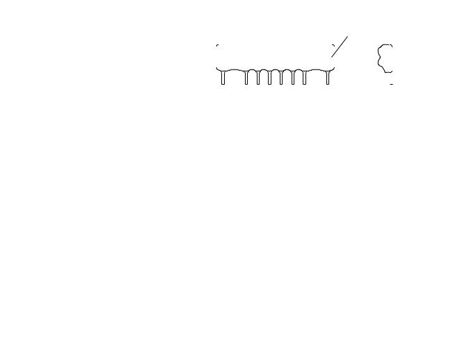
Fig.1 |
Simplified outline. |
|
|
|
||||||
8 |
output/supply (+) |
|
|
|
|
|
|
|
|
||||||||
|
|
|
|
|
|
|
|
|
|
|
|
|
|
|
|
||
|
|
|
|
|
|
|
|
|
|
|
|
|
|
|
|
|
|
QUICK REFERENCE DATA |
|
|
|
|
|
|
|
|
|
|
|
|
|
|
|||
|
|
|
|
|
|
|
|
|
|
|
|
||||||
SYMBOL |
PARAMETER |
|
|
CONDITIONS |
|
MIN. |
|
TYP. |
|
MAX. |
UNIT |
||||||
|
|
|
|
|
|
|
|
|
|
|
|
|
|
|
|||
f |
frequency range |
|
|
|
|
|
40 |
|
|
- |
|
|
860 |
MHz |
|||
|
|
|
|
|
|
|
|
|
|
|
|
|
|
|
|
||
ZS, ZL |
source and load impedance |
|
|
|
|
|
- |
|
|
|
75 |
|
|
- |
W |
||
GT |
transducer gain = ïS21ï2 |
|
|
|
|
|
- |
|
|
|
29 |
|
|
- |
dB |
||
DGT |
flatness of frequency response |
|
|
|
|
|
- |
|
|
|
1 |
|
|
- |
dB |
||
Vo(rms) |
output voltage (RMS value) |
dim = -60 dB; |
|
|
|
|
|
|
|
|
|
|
|
||||
|
|
|
|
3rd order intermodulation (3-tone) |
|
|
|
|
|
|
|
|
|
||||
|
|
|
|
VHF |
|
|
- |
|
|
|
103 |
|
|
- |
dBmV |
||
|
|
|
|
UHF |
|
|
- |
|
|
|
105 |
|
|
- |
dBmV |
||
|
|
|
|
|
|
|
|
|
|
|
|
|
|
|
|
||
F |
noise figure |
|
|
|
|
|
- |
|
|
|
3.6 |
|
|
- |
dB |
||
VB |
DC supply voltage |
|
|
|
|
|
10.8 |
|
12 |
|
|
13.2 |
V |
||||
Tamb |
ambient operating temperature |
|
|
|
|
|
-20 |
|
- |
|
|
+70 |
°C |
||||
1995 Nov 28 |
2 |
Philips Semiconductors |
Product specification |
|
|
Wideband amplifier module |
OM2063 |
|
|
CIRCUIT DIAGRAM AND PRINTED-CIRCUIT BOARD
|
C1 |
|
C4 |
C5 |
R8 |
R10 |
R13 |
|
|
|
|
|
|
|
8 |
R1 |
R3 |
|
|
|
|
|
C6 |
|
|
|
|
|
|
|
|
|
|
TR1 |
|
|
|
TR2 |
TR3 |
|
|
R4 |
|
R7 |
|
R9 |
R14 |
1 |
|
|
|
|
|
R11 |
R12 |
|
|
|
|
|
|
||
R2 |
C2 |
R5 |
R6 |
|
|
|
C7 |
|
|
|
|
|
|
|
|
2,3 |
|
|
|
|
|
|
5,6,7 |
|
|
C3 |
|
|
|
|
MGD020 |
|
|
|
4 |
|
|
|
|
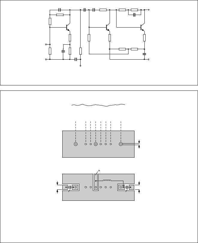
Fig.2 Circuit diagram.
|
|
|
|
|
|
|
|
|
|
|
|
|
|
|
|
|
1 |
|
|
|
|
|
|
|
|
|
|
|
|
|
|
|
8 |
|
|
|
|
|
|
|
|
|
|
|
|
|
|
|
|
|
|
1 |
|
(8x) |
|
TOP VIEW |
|
L |
75 Ω |
75 Ω |
track |
track |
C |
C |
|
MGD061 |
|
BOTTOM VIEW |
L > 5 μH; e.g. catalogue No. 3122 108 20150, or 27 turns enamelled 0.3 mm copper wire wound on a ferrite core (material 4B1; catalogue No. 3122 104 91110) with a diameter of 1.6 mm.
C > 220 pF ceramic capacitor.
Fig.3 Printed-circuit board holes and tracks.
1995 Nov 28 |
3 |

Philips Semiconductors |
|
|
|
|
Product specification |
||||
|
|
|
|
|
|
|
|
|
|
Wideband amplifier module |
|
|
|
|
|
OM2063 |
|||
|
|
|
|
|
|
|
|
|
|
LIMITING VALUES |
|
|
|
|
|
|
|
|
|
In accordance with the Absolute Maximum Rating System (IEC 134). |
|
|
|
|
|
|
|
||
|
|
|
|
|
|
|
|
|
|
SYMBOL |
PARAMETER |
MIN. |
|
MAX. |
|
UNIT |
|||
|
|
|
|
|
|
|
|
|
|
VB |
DC supply voltage |
|
- |
|
|
15 |
|
V |
|
PIM |
peak incident powers on pins 1 and 8 |
- |
|
|
100 |
|
mW |
||
Tamb |
ambient operating temperature |
|
-20 |
|
|
+70 |
|
°C |
|
Tstg |
storage temperature |
|
-40 |
|
|
+125 |
°C |
||
CHARACTERISTICS |
|
|
|
|
|
|
|
|
|
|
|
|
|
|
|
|
|
||
SYMBOL |
PARAMETER |
CONDITIONS |
MIN. |
|
TYP. |
MAX. |
UNIT |
||
|
|
|
|
|
|
|
|
|
|
Measuring conditions |
|
|
|
|
|
|
|
|
|
|
|
|
|
|
|
|
|
|
|
Tamb |
ambient operating temperature |
|
- |
|
25 |
|
- |
|
°C |
VB |
DC supply voltage |
|
- |
|
12 |
|
- |
|
V |
ZS |
source impedance |
|
- |
|
75 |
|
- |
|
W |
ZL |
load impedance |
|
- |
|
75 |
|
- |
|
W |
Z0 |
characteristic impedance of |
|
- |
|
75 |
|
- |
|
W |
|
HF connections |
|
|
|
|
|
|
|
|
|
|
|
|
|
|
|
|
|
|
f |
frequency range |
|
40 |
|
- |
|
860 |
|
MHz |
|
|
|
|
|
|
|
|
|
|
Performance |
|
|
|
|
|
|
|
|
|
|
|
|
|
|
|
|
|
|
|
IB |
supply current |
|
- |
|
52 |
|
- |
|
mA |
GT |
transducer gain = ïS21ï2 |
|
- |
|
29 |
|
- |
|
dB |
DGT |
flatness of frequency response |
|
- |
|
1 |
|
1.5 |
|
dB |
VSWRin |
individual maximum VSWR |
input; note 1 |
- |
|
2.3 |
- |
|
|
|
VSWRout |
individual maximum VSWR |
output; note 1 |
- |
|
1.4 |
- |
|
|
|
ïS12ï2 |
back attenuation |
f = 100 MHz |
- |
|
46 |
|
- |
|
dB |
|
|
f = 860 MHz |
- |
|
41 |
|
- |
|
dB |
|
|
|
|
|
|
|
|
|
|
Vo(rms) |
output voltage (RMS value) |
dim = -60 dB; |
|
|
|
|
|
|
|
|
|
3rd order intermodulation (3-tone) |
|
|
|
|
|
|
|
|
|
VHF |
- |
|
103 |
- |
|
dBmV |
|
|
|
UHF |
- |
|
105 |
- |
|
dBmV |
|
|
|
|
|
|
|
|
|
|
|
F |
noise figure |
|
- |
|
3.6 |
- |
|
dB |
|
|
|
|
|
|
|
|
|
|
|
Operating conditions |
|
|
|
|
|
|
|
|
|
|
|
|
|
|
|
|
|
|
|
Tamb |
ambient operating temperature |
|
-20 |
|
- |
|
+70 |
|
°C |
VB |
DC supply voltage |
|
10.8 |
|
12 |
|
13.2 |
|
V |
f |
frequency range |
|
40 |
|
- |
|
860 |
|
MHz |
ZS |
source impedance |
|
- |
|
75 |
|
- |
|
W |
ZL |
load impedance |
|
- |
|
75 |
|
- |
|
W |
Note
1. Highest value (for sample) occurring in the frequency range.
1995 Nov 28 |
4 |
Philips Semiconductors |
Product specification |
|
|
Wideband amplifier module |
OM2063 |
|
|
MEA199
34
S21 (dB)
32
30
28
26
0 |
200 |
400 |
600 |
800 |
1000 |
|
|
|
|
f |
(MHz) |
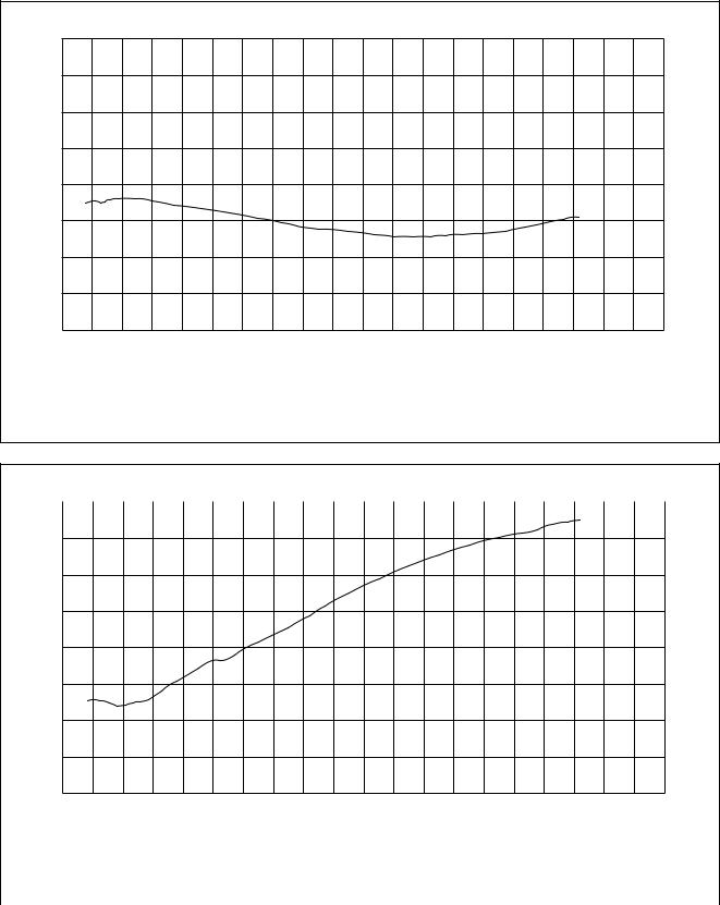
Gain over entire frequency range.
Z0 = 75 Ω.
Fig.4 Transducer gain as a function of frequency.
−41 |
MEA200 |
|
S12
(dB)
−43
−45
−47
−49
0 |
200 |
400 |
600 |
800 |
1000 |
|
|
|
|
f |
(MHz) |
Gain over entire frequency range.
Z0 = 75 Ω.
Fig.5 |
Back attenuation as a function of frequency. |
|
|
1995 Nov 28 |
5 |