Материал: 9689

Philips Semiconductors Product specification
Thyristors |
|
|
|
|
|
|
|
|
|
|
|
|
|
|
|
|
|
|
|
|
|
|
|
|
|
|
|
BT168W series |
|
||||||||||||||||
logic level for RCD/ GFI applications |
|
|
|
|
|
|
|
|
|
|
|
|
|
|
|
|
|
|
|
|
|
|
|
|
|
|
|
|
|||||||||||||||||
|
|
|
|
|
|
|
|
|
|
|
|
|
|
|
|
|
|
|
|
|
|
|
|||||||||||||||||||||||
GENERAL DESCRIPTION |
QUICK REFERENCE DATA |
|
|
|
|
|
|
|
|
|
|
|
|
|
|
|
|
|
|
|
|
|
|||||||||||||||||||||||
|
|
|
|
|
|
|
|
|
|
|
|
|
|
||||||||||||||||||||||||||||||||
Glass |
passivated, sensitive gate |
|
SYMBOL |
|
PARAMETER |
|
|
MAX. |
MAX. |
MAX. |
MAX. |
UNIT |
|
||||||||||||||||||||||||||||||||
thyristors in a plastic envelope |
|
|
|
|
|
|
|
|
|
|
|
|
|
|
|
|
|
|
|
|
|
|
|
|
|
|
|
|
|
|
|
|
|
|
|
|
|||||||||
|
|
|
|
|
|
|
|
|
|
|
|
|
|
BT168 |
|
|
BW |
|
|
DW |
|
|
EW |
|
|
|
GW |
|
|
|
|
|
|
||||||||||||
suitable |
|
|
for |
surface |
mounting, |
|
|
|
|
|
|
|
|
|
|
|
|
|
|
|
|
|
|
|
|
|
|
|
|
|
|
|
|
|
|||||||||||
intended for use in Residual Current |
|
VDRM, |
|
Repetitive peak |
|
200 |
|
400 |
|
500 |
|
600 |
|
|
|
V |
|
||||||||||||||||||||||||||||
Devices/ Ground |
Fault Interrupters |
|
VRRM |
|
off-state voltages |
|
|
|
|
|
|
|
|
|
|
|
|
|
|
|
|
|
|
|
|
|
|||||||||||||||||||
(RCD/ GFI) |
applications |
where a |
|
IT(AV) |
|
Average on-state |
|
0.6 |
|
0.6 |
|
0.6 |
|
0.6 |
|
|
|
A |
|
||||||||||||||||||||||||||
minimum IGT limit is needed. These |
|
|
|
|
|
|
|
current |
|
|
|
|
|
|
|
|
|
|
|
|
|
|
|
|
|
|
|
|
|
|
|
|
|
|
|||||||||||
devices may be interfaced directly to |
|
IT(RMS) |
|
RMS on-state current |
|
1 |
|
1 |
|
1 |
|
1 |
|
|
|
A |
|
||||||||||||||||||||||||||||
microcontrollers, |
logic |
integrated |
|
ITSM |
|
Non-repetitive peak |
|
8 |
|
8 |
|
8 |
|
8 |
|
|
|
A |
|
||||||||||||||||||||||||||
circuits and other low power gate |
|
|
|
|
|
|
|
on-state current |
|
|
|
|
|
|
|
|
|
|
|
|
|
|
|
|
|
|
|
|
|
||||||||||||||||
trigger circuits. |
|
|
|
|
|
|
|
|
|
|
|
|
|
|
|
|
|
|
|
|
|
|
|
|
|
|
|
|
|
|
|
|
|
|
|
|
|
|
|
|
|||||
PINNING - SOT223 |
|
|
|
PIN CONFIGURATION |
|
|
SYMBOL |
|
|
|
|
|
|
|
|
|
|
|
|
|
|||||||||||||||||||||||||
|
|
|
|
|
|
|
|
|
|
|
|
|
|
|
|
|
|
|
|
|
|
|
|
|
|
|
|
|
|
|
|
|
|
|
|
|
|
|
|
|
|
|
|||
|
PIN |
|
|
|
DESCRIPTION |
|
|
|
|
|
|
|
|
|
|
|
4 |
|
|
|
|
|
|
|
|
|
|
|
|
|
|
|
|
|
|
|
|
|
|
|
|
||||
|
|
|
|
|
|
|
|
|
|
|
|
|
|
|
|
|
|
|
|
|
|
|
|
|
|
|
|
|
|
|
|
|
|
|
|
|
|||||||||
|
|
|
|
|
|
|
|
|
|
|
|
|
|
|
|
|
|
|
|
|
|
|
|
|
|
|
|
|
|
|
|
|
|
|
|
|
|
|
|
|
|
|
|
||
1 |
|
|
cathode |
|
|
|
|
|
|
|
|
|
|
|
|
|
|
|
|
|
|
|
|
|
|
|
|
a |
|
|
|
|
|
|
|
|
|
|
k |
|
|||||
|
|
|
|
|
|
|
|
|
|
|
|
|
|
|
|
|
|
|
|
|
|
|
|
|
|
|
|
|
|
|
|
|
|
|
|
|
|||||||||
|
|
|
|
|
|
|
|
|
|
|
|
|
|
|
|
|
|
|
|
|
|
|
|
|
|
|
|
|
|
|
|
||||||||||||||
2 |
|
|
anode |
|
|
|
|
|
|
|
|
|
|
|
|
|
|
|
|
|
|
|
|
|
|
|
|
|
|
|
|
|
|
|
|
|
|
|
|
|
|
|
|
||
3 |
|
|
gate |
|
|
|
|
|
|
|
|
|
|
|
|
|
|
|
|
|
|
|
|
|
|
|
|
|
|
|
|
|
|
|
|
|
g |
|
|
|
|
|
|
||
|
|
|
|
|
|
|
|
|
|
|
|
|
|
|
|
|
|
|
|
|
|
|
|
|
|
|
|
|
|
|
|
|
|
|
|
|
|
|
|||||||
|
|
|
|
|
|
|
|
|
|
|
1 |
|
2 |
|
|
3 |
|
|
|
|
|
|
|
|
|
|
|
|
|
|
|
|
|
|
|
||||||||||
|
tab |
|
|
anode |
|
|
|
|
|
|
|
|
|
|
|
|
|
|
|
|
|
|
|
|
|
|
|
|
|
|
|
|
|
|
|
|
|||||||||
|
|
|
|
|
|
|
|
|
|
|
|
|
|
|
|
|
|
|
|
|
|
|
|
|
|
|
|
|
|
|
|
||||||||||||||
|
|
|
|
|
|
|
|
|
|
|
|
|
|
|
|
|
|
|
|
|
|
|
|
|
|
|
|
|
|
|
|
|
|
|
|
|
|
|
|
|
|
|
|||
|
|
|
|
|
|
|
|
|
|
|
|
|
|
|
|
|
|
|
|
|
|
|
|
|
|
|
|
|
|
|
|
|
|
|
|
|
|
|
|
|
|
|
|
|
|
LIMITING VALUES
Limiting values in accordance with the Absolute Maximum System (IEC 134).
SYMBOL |
PARAMETER |
CONDITIONS |
MIN. |
|
MAX. |
|
UNIT |
||||
|
|
|
|
|
|
B |
D |
|
E |
G |
|
V |
, V |
RRM |
Repetitive peak off-state |
|
- |
2001 |
4001 |
|
5001 |
6001 |
V |
DRM |
|
voltages |
|
|
|
|
|
|
|
|
|
|
|
|
|
|
|
|
|
|
|
|
|
|
|
|
|
|
|
|
|
|
|
|
|
IT(AV) |
|
|
Average on-state current |
half sine wave; |
- |
|
0.63 |
|
A |
||
IT(RMS) |
|
|
Tsp ≤ 112 ˚C |
|
|
|
|
|
|
|
|
|
RMS on-state current |
all conduction angles |
- |
|
|
1 |
|
A |
|||
ITSM |
|
|
Non-repetitive peak |
t = 10 ms |
- |
|
|
8 |
|
A |
|
|
|
|
on-state current |
t = 8.3 ms |
- |
|
|
9 |
|
A |
|
|
|
|
|
half sine wave; |
|
|
|
|
|
|
|
|
|
|
|
Tj = 125 ˚C prior to |
|
|
|
|
|
|
|
|
|
|
|
surge; with reapplied |
|
|
|
|
|
|
|
I2t |
|
|
I2t for fusing |
VDRM(max) |
- |
|
0.32 |
|
A2s |
||
|
|
t = 10 ms |
|
|
|||||||
dIT/dt |
|
Repetitive rate of rise of |
ITM = 2 A; IG = 10 mA; |
- |
|
|
50 |
|
A/μs |
||
|
|
|
on-state current after |
dIG/dt = 100 mA/μs |
|
|
|
|
|
|
|
|
|
|
triggering |
|
|
|
|
|
|
|
|
IGM |
|
|
Peak gate current |
|
- |
|
|
1 |
|
A |
|
VGM |
|
|
Peak gate voltage |
|
- |
|
|
5 |
|
V |
|
VRGM |
|
Peak reverse gate voltage |
|
- |
|
|
5 |
|
V |
||
PGM |
|
|
Peak gate power |
|
- |
|
|
2 |
|
W |
|
PG(AV) |
|
Average gate power |
over any 20 ms period |
- |
|
|
0.1 |
|
W |
||
Tstg |
|
|
Storage temperature |
|
-40 |
|
150 |
|
˚C |
||
Tj |
|
|
Operating junction |
|
- |
|
125 |
|
˚C |
||
|
|
|
temperature |
|
|
|
|
|
|
|
|
1 Although not recommended, off-state voltages up to 800V may be applied without damage, but the thyristor may switch to the on-state. The rate of rise of current should not exceed 15 A/μs.
February 1996 |
1 |
Rev 1.000 |

Philips Semiconductors Product specification
Thyristors |
|
|
BT168W series |
|
|||
logic level for RCD/ GFI Applications |
|
|
|
|
|
||
|
|
|
|
|
|
|
|
THERMAL RESISTANCES |
|
|
|
|
|
|
|
|
|
|
|
|
|
|
|
SYMBOL |
PARAMETER |
CONDITIONS |
MIN. |
TYP. |
MAX. |
UNIT |
|
|
|
|
|
|
|
|
|
Rth j-sp |
Thermal resistance |
|
- |
- |
15 |
K/W |
|
|
junction to solder point |
|
|
|
|
|
|
Rth j-a |
Thermal resistance |
pcb mounted, minimum footprint |
- |
156 |
- |
K/W |
|
|
junction to ambient |
pcb mounted, pad area as in fig:14 |
- |
70 |
- |
K/W |
|
STATIC CHARACTERISTICS |
|
|
|
|
|
|
|
Tj = 25 ˚C unless otherwise stated |
|
|
|
|
|
|
|
SYMBOL |
PARAMETER |
CONDITIONS |
MIN. |
TYP. |
MAX. |
UNIT |
|
|
|
|
|
|
|
|
|
IGT |
Gate trigger current |
VD = 12 V; IT = 10 mA; gate open circuit |
20 |
50 |
200 |
μA |
|
IL |
Latching current |
VD = 12 V; IGT = 0.5 mA; RGK = 1 kΩ |
- |
2 |
6 |
mA |
|
IH |
Holding current |
VD = 12 V; IGT = 0.5 mA; RGK = 1 kΩ |
- |
2 |
5 |
mA |
|
VT |
On-state voltage |
IT = 2 A |
- |
1.35 |
1.5 |
V |
|
VGT |
Gate trigger voltage |
VD = 12 V; IT = 10 mA; gate open circuit |
- |
0.5 |
0.8 |
V |
|
|
|
VD = VDRM(max); IT = 10 mA; Tj = 125 ˚C; |
0.2 |
0.3 |
- |
V |
|
|
|
gate open circuit |
|
|
|
|
|
ID, IR |
Off-state leakage current |
VD = VDRM(max); VR = VRRM(max); Tj = 125 ˚C; |
- |
0.05 |
0.1 |
mA |
|
|
|
RGK = 1 kΩ |
|
|
|
|
|
DYNAMIC CHARACTERISTICS |
|
|
|
|
|
|
|
Tj = 25 ˚C unless otherwise stated |
|
|
|
|
|
|
|
SYMBOL |
PARAMETER |
CONDITIONS |
MIN. |
TYP. |
MAX. |
UNIT |
|
|
|
|
|
|
|
|
|
dVD/dt |
Critical rate of rise of |
VDM = 67% VDRM(max); Tj = 125 ˚C; |
- |
25 |
- |
V/μs |
|
|
off-state voltage |
exponential waveform; RGK = 1 kΩ |
|
|
|
μs |
|
tgt |
Gate controlled turn-on |
ITM = 2 A; VD = VDRM(max); IG = 10 mA; |
- |
2 |
- |
|
|
|
time |
dIG/dt = 0.1 A/μs |
|
|
|
μs |
|
tq |
Circuit commutated |
VD = 67% VDRM(max); Tj = 125 ˚C; |
- |
100 |
- |
|
|
|
turn-off time |
ITM = 1.6 A; VR = 35 V; dITM/dt = 30 A/μs; |
|
|
|
|
|
|
|
dVD/dt = 2 V/μs; RGK = 1 kΩ |
|
|
|
|
|
February 1996 |
2 |
Rev 1.000 |
Philips Semiconductors |
Product specification |
|
|
Thyristors |
BT168W series |
logic level for RCD/ GFI Applications |
|
|
|
1 |
Ptot / W |
|
BT169W |
|
Tsp(max) / C110 |
|||
|
|
conduction |
form |
|
|
|
a = 1.57 |
|
|
|
angle |
factor |
|
|
|
|
|
|
|
degrees |
a |
|
|
1.9 |
|
|
0.8 |
|
30 |
4 |
|
|
|
113 |
|
|
60 |
2.8 |
|
|
2.2 |
|
||
|
|
|
|
|
|
|||
|
|
90 |
2.2 |
|
2.8 |
|
|
|
|
|
120 |
1.9 |
|
|
|
|
|
0.6 |
|
180 |
1.57 |
4 |
|
|
|
116 |
|
|
|
|
|
|
|||
|
|
|
|
|
|
|
|
|
0.4 |
|
|
|
|
|
|
|
119 |
0.2 |
|
|
|
|
|
|
|
122 |
0 |
0 |
0.1 |
0.2 |
0.3 |
0.4 |
0.5 |
0.6 |
125 |
|
0.7 |
|||||||
|
|
|
|
IF(AV) / A |
|
|
|
|
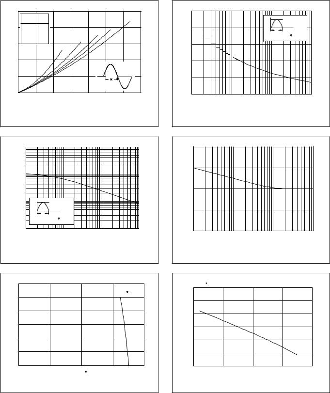
Fig.1. Maximum on-state dissipation, Ptot, versus |
||||||||
average on-state current, IT(AV), where a = form |
||||||||
|
|
|
factor = IT(RMS)/ IT(AV). |
|
|
|||
1000 |
ITSM / A |
|
BT169 |
|
100 |
|
|
|
|
10 |
IT |
ITSM |
|
|
|
T |
time |
|
|
|
Tj initial = 125 C max |
|
|
|
1 |
|
100us |
1ms |
10ms |
10us |
||||
|
|
|
T / s |
|
Fig.2. Maximum permissible non-repetitive peak on-state current ITSM, versus pulse width tp, for sinusoidal currents, tp ≤ 10ms.
1.2 |
IT(RMS) / A |
|
BT134W |
|
|
1 |
|
|
|
|
112 C |
|
|
|
|
|
|
0.8 |
|
|
|
|
|
0.6 |
|
|
|
|
|
0.4 |
|
|
|
|
|
0.2 |
|
|
|
|
|
0 |
|
0 |
50 |
100 |
150 |
-50 |
|||||
|
|
|
Tsp / C |
|
|
Fig.3. Maximum permissible rms current IT(RMS) , versus solder point temperature Tsp.
10 |
ITSM / A |
|
BT169 |
|
|
|
|
IT |
ITSM |
8 |
|
|
T |
time |
|
|
|
||
|
|
|
Tj initial = 125 C max |
|
6 |
|
|
|
|
4 |
|
|
|
|
2 |
|
|
|
|
0 |
1 |
10 |
100 |
1000 |
|
|
Number of half cycles at 50Hz |
|
|
Fig.4. Maximum permissible non-repetitive peak on-state current ITSM, versus number of cycles, for sinusoidal currents, f = 50 Hz.
IT(RMS) / A |
|
BT134W |
|
2 |
|
|
|
1.5 |
|
|
|
1 |
|
|
|
0.5 |
|
|
|
0 |
0.1 |
1 |
10 |
0.01 |
surge duration / s
Fig.5. Maximum permissible repetitive rms on-state
current IT(RMS), versus surge duration, for sinusoidal currents, f = 50 Hz; Tsp ≤ 112˚C.
|
VGT(Tj) |
|
BT151 |
|
|
1.6 |
VGT(25 C) |
|
|
|
|
1.4 |
|
|
|
|
|
1.2 |
|
|
|
|
|
1 |
|
|
|
|
|
0.8 |
|
|
|
|
|
0.6 |
|
|
|
|
|
0.4 |
|
0 |
50 |
100 |
150 |
-50 |
|||||
|
|
|
Tj / C |
|
|
Fig.6. Normalised gate trigger voltage VGT(Tj)/ VGT(25˚C), versus junction temperature Tj.
February 1996 |
3 |
Rev 1.000 |
Philips Semiconductors |
Product specification |
|
|
Thyristors |
BT168W series |
logic level for RCD/ GFI Applications |
|
|
|
|
IGT(Tj) |
|
BT169 |
|
|
3 |
IGT(25 C) |
|
|
|
|
2.5 |
|
|
|
|
|
2 |
|
|
|
|
|
1.5 |
|
|
|
|
|
1 |
|
|
|
|
|
0.5 |
|
|
|
|
|
0 |
|
0 |
50 |
100 |
150 |
-50 |
|||||
|
|
|
Tj / C |
|
|
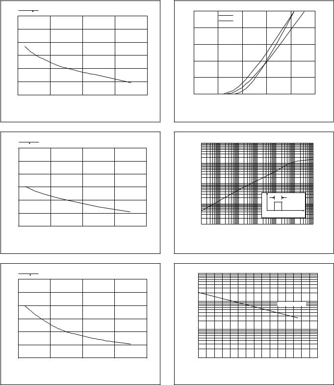
Fig.7. Normalised gate trigger current IGT(Tj)/ IGT(25˚C), versus junction temperature Tj.
|
IL(Tj) |
|
|
|
|
3 |
IL(25 C) |
BT169 |
|
|
|
|
|
|
|
|
|
2.5 |
|
|
|
|
|
2 |
|
|
|
|
|
1.5 |
|
|
|
|
|
1 |
|
|
|
|
|
0.5 |
|
|
|
|
|
0 |
|
0 |
50 |
100 |
150 |
-50 |
|||||
|
|
|
Tj / C |
|
|
Fig.8. |
Normalised latching current IL(Tj)/ IL(25˚C), |
||||
|
versus junction temperature Tj, RGK = 1 kΩ. |
|
|||
|
IH(Tj) |
|
|
|
|
3 |
IH(25 C) |
BT169 |
|
|
|
2.5 |
|
|
|
|
|
2 |
|
|
|
|
|
1.5 |
|
|
|
|
|
1 |
|
|
|
|
|
0.5 |
|
|
|
|
|
0 |
|
0 |
50 |
100 |
150 |
-50 |
|||||
|
|
|
Tj / C |
|
|
Fig.9. Normalised holding current IH(Tj)/ IH(25˚C), versus junction temperature Tj, RGK = 1 kΩ.
IT / A |
BT169W |
5
Tj = 125 C
Tj = 25 C
4Vo = 1.0 V
Rs = 0.27 Ohms
3 |
|
|
|
|
|
2 |
|
typ |
|
max |
|
|
|
|
|
|
|
1 |
|
|
|
|
|
0 0 |
0.5 |
1 |
1.5 |
2 |
2.5 |
|
|
VT / V |
|
|
|
Fig.10. Typical and maximum on-state characteristic.
100 Zth j-sp (K/W) |
|
BT169W |
|
|
|
|
10 |
|
|
|
|
|
|
1 |
|
|
|
|
|
|
|
|
|
P |
t p |
|
|
|
|
|
D |
|
|
|
0.1 |
|
|
|
|
|
|
|
|
|
|
|
|
t |
0.01 |
0.1ms |
1ms |
10ms |
0.1s |
1s |
10s |
10us |
||||||
|
|
|
tp / s |
|
|
|
Fig.11. Transient thermal impedance Zth j-sp, versus pulse width tp.
1000 |
dVD/dt (V/us) |
|
|
|
100 |
|
|
RGK = 1 kohms |
|
|
|
|
|
|
10 |
|
|
|
|
1 |
0 |
50 |
100 |
150 |
|
|
|
Tj / C |
|
Fig.12. Typical, critical rate of rise of off-state voltage, dVD/dt versus junction temperature Tj.
February 1996 |
4 |
Rev 1.000 |
Philips Semiconductors Product specification
Thyristors |
BT168W series |
logic level for RCD/ GFI Applications |
|
|
|
MOUNTING INSTRUCTIONS |
PRINTED CIRCUIT BOARD |
|
Dimensions in mm. |
Dimensions in mm. |
3.8 |
|
36 |
|
|
|
min |
|
|
1.5 |
|
18 |
min |
|
|
|
|
|
|
60 |
|
|
4.6 |
4.5 |
|
9 |
|
2.3 |
6.3 |
|
1.5 |
|
|
min |
10 |
|
|
|
|
(3x) |
|
|
1.5 |
|
|
min |
|
|
4.6 |
|
7 |
|
|
15 |
|
50 |
|
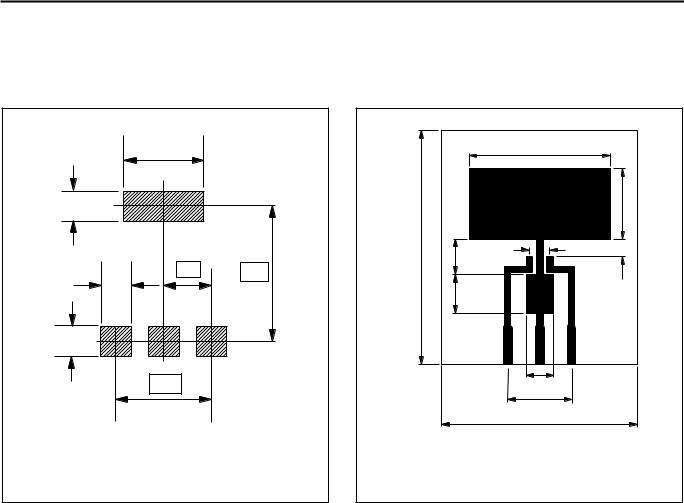
Fig.13. soldering pattern for surface mounting |
Fig.14. PCB for thermal resistance and power rating |
SOT223. |
for SOT223. |
|
PCB: FR4 epoxy glass (1.6 mm thick), copper |
|
laminate (35 μm thick). |
February 1996 |
5 |
Rev 1.000 |