Материал: BUH100RE
MOTOROLA
SEMICONDUCTOR TECHNICAL DATA
Order this document by BUH100/D
BUH100
Designer's Data Sheet
SWITCHMODE NPN Silicon
Planar Power Transistor
POWER TRANSISTOR
10 AMPERES
700 VOLTS
100 WATTS
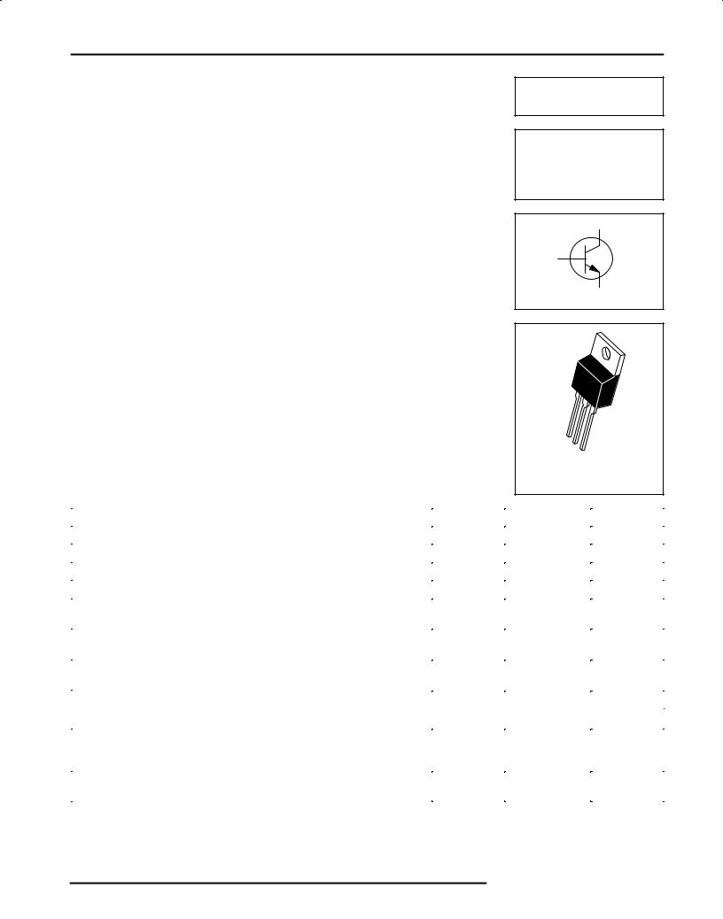
The BUH100 has an application specific state±of±art die designed for use in 100 Watts Halogen electronic transformers.
This power transistor is specifically designed to sustain the large inrush current during either the start±up conditions or under a short circuit across the load.
This High voltage/High speed product exhibits the following main features:
•Improved Efficiency Due to the Low Base Drive Requirements:
ÐHigh and Flat DC Current Gain h FE
ÐFast Switching
•Robustness Thanks to the Technology Developed to Manufacture this Device
•Motorola ª6 SIGMAº Philosophy Provides Tight and Reproducible Parametric Distributions
MAXIMUM RATINGS
CASE 221A±06
TO±220AB
Rating |
Symbol |
Value |
Unit |
|
|
|
|
Collector±Emitter Sustaining Voltage |
VCEO |
400 |
Vdc |
Collector±Base Breakdown Voltage |
VCBO |
700 |
Vdc |
Collector±Emitter Breakdown Voltage |
VCES |
700 |
Vdc |
Emitter±Base Voltage |
VEBO |
10 |
Vdc |
Collector Current Ð Continuous |
IC |
10 |
Adc |
Ð Peak (1) |
ICM |
20 |
|
Base Current Ð Continuous |
IB |
4 |
Adc |
Base Current Ð Peak (1) |
IBM |
10 |
|
*Total Device Dissipation @ TC = 25_C |
PD |
100 |
Watt |
*Derate above 25°C |
|
0.8 |
W/_C |
|
|
|
|
Operating and Storage Temperature |
TJ, Tstg |
± 65 to 150 |
_C |
THERMAL CHARACTERISTICS
Thermal Resistance |
|
|
_C/W |
Ð Junction to Case |
RqJC |
1.25 |
|
Ð Junction to Ambient |
RqJA |
62.5 |
|
Maximum Lead Temperature for Soldering Purposes: |
TL |
260 |
_C |
1/8″ from case for 5 seconds |
|
|
|
|
|
|
|
(1) Pulse Test: Pulse Width = 5 ms, Duty Cycle ≤ 10%. |
|
|
|
Designer's and SWITCHMODE are trademarks of Motorola, Inc.
Designer's Data for ªWorst Caseº Conditions Ð The Designer 's Data Sheet permits the design of most circuits entirely from the information presented. SOA Limit curves Ð representing boundaries on device characteristics Ð are given to facilitate ªworst caseº design.
Motorola, Inc. 1995

BUH100
ELECTRICAL CHARACTERISTICS (TC = 25°C unless otherwise noted)
|
|
Characteristic |
|
Symbol |
Min |
Typ |
Max |
Unit |
|
|
|
|
|
|
|
|
|
OFF CHARACTERISTICS |
|
|
|
|
|
|
|
|
|
|
|
|
|
|
|
|
|
Collector±Emitter Sustaining Voltage |
|
VCEO(sus) |
400 |
460 |
|
Vdc |
||
(IC = 100 mA, L = 25 mH) |
|
|
|
|
|
|
||
Collector±Base Breakdown Voltage |
|
VCBO |
700 |
860 |
|
Vdc |
||
(ICBO = 1 mA) |
|
|
|
|
|
|
|
|
Emitter±Base Breakdown Voltage |
|
VEBO |
10 |
12.5 |
|
Vdc |
||
(IEBO = 1 mA) |
|
|
|
|
|
|
|
|
Collector Cutoff Current |
|
|
ICEO |
|
|
100 |
μAdc |
|
(VCE = Rated VCEO, IB = 0) |
|
|
|
|
|
|
||
Collector Cutoff Current |
|
@ TC = 25°C |
ICES |
|
|
100 |
μAdc |
|
(VCE = Rated VCES, VEB = 0) |
@ TC = 125°C |
|
|
|
1000 |
|
||
Collector Base Current |
|
@ TC = 25°C |
ICBO |
|
|
100 |
μAdc |
|
(VCB = Rated VCBO, VEB = 0) |
@ TC = 125°C |
|
|
|
1000 |
|
||
Emitter±Cutoff Current |
|
|
IEBO |
|
|
100 |
μAdc |
|
(VEB = 9 Vdc, IC = 0) |
|
|
|
|
|
|
|
|
ON CHARACTERISTICS |
|
|
|
|
|
|
|
|
|
|
|
|
|
|
|
|
|
Base±Emitter Saturation Voltage |
@ TC = 25°C |
VBE(sat) |
|
1 |
1.1 |
Vdc |
||
(IC = 5 Adc, IB = 1 Adc) |
|
|
|
|
|
|
|
|
Collector±Emitter Saturation Voltage |
@ TC = 25°C |
VCE(sat) |
|
0.37 |
0.6 |
Vdc |
||
(IC = 5 Adc, IB = 1 Adc) |
|
@ TC = 125°C |
|
|
0.37 |
0.6 |
|
|
(IC = 7 Adc, IB = 1.5 Adc) |
@ TC = 25°C |
|
|
0.5 |
0.75 |
Vdc |
||
|
|
|
@ TC = 125°C |
|
|
0.6 |
1.5 |
|
DC Current Gain (IC = 1 Adc, VCE = 5 Vdc) |
@ TC = 25°C |
hFE |
15 |
24 |
|
Ð |
||
|
|
|
@ TC = 125°C |
|
16 |
28 |
|
|
DC Current Gain (IC = 5 Adc, VCE = 5 Vdc) |
@ TC = 25°C |
|
10 |
15 |
|
Ð |
||
|
|
|
@ TC = 125°C |
|
10 |
14.5 |
|
|
DC Current Gain (IC = 7 Adc, VCE = 5 Vdc) |
@ TC = 25°C |
|
8 |
12 |
|
Ð |
||
|
|
|
@ TC = 125°C |
|
7 |
10.5 |
|
|
DC Current Gain (IC = 10 Adc, VCE = 5 Vdc) |
@ TC = 25°C |
|
6 |
9.5 |
|
Ð |
||
|
|
|
@ TC = 125°C |
|
4 |
8 |
|
|
DYNAMIC SATURATION VOLTAGE |
|
|
|
|
|
|
||
|
|
|
|
|
|
|
|
|
Dynamic Saturation |
|
IC = 5 Adc, IB1 = 1 Adc |
@ TC = 25°C |
VCE(dsat) |
|
1.1 |
|
V |
Voltage: |
|
VCC = 300 V |
|
|
|
|
|
|
|
@ TC = 125°C |
|
|
2.1 |
|
V |
||
μ |
|
|
|
|
||||
Determined 3 s after |
|
|
|
|
|
|
|
|
rising IB1 reaches |
|
IC = 7.5 Adc, IB1 = 1.5 Adc |
@ TC = 25°C |
|
|
1.7 |
|
V |
90% of final IB1 |
|
|
|
|
|
|
|
|
|
VCC = 300 V |
° |
|
|
5 |
|
V |
|
(See Figure 19) |
|
|
|
|
||||
|
|
@ TC = 125 C |
|
|
|
|||
DYNAMIC CHARACTERISTICS |
|
|
|
|
|
|
||
|
|
|
|
|
|
|
|
|
Current Gain Bandwidth |
|
|
fT |
|
23 |
|
MHz |
|
(IC = 1 Adc, VCE = 10 Vdc, f = 1 MHz) |
|
|
|
|
|
|
||
Output Capacitance |
|
|
Cob |
|
100 |
150 |
pF |
|
(VCB = 10 Vdc, IE = 0, f = 1 MHz) |
|
|
|
|
|
|
||
Input Capacitance |
|
|
Cib |
|
1300 |
1750 |
pF |
|
(VEB = 8 Vdc, f = 1 MHz) |
|
|
|
|
|
|
|
|
2 |
Motorola Bipolar Power Transistor Device Data |

|
|
|
|
|
|
|
|
|
|
|
BUH100 |
|
ELECTRICAL CHARACTERISTICS (TC = 25°C unless otherwise noted) |
|
|
|
|
|
|
|
|||||
|
|
|
|
|
|
|
|
|
|
|
|
|
|
Characteristic |
|
|
|
Symbol |
|
Min |
Typ |
Max |
|
Unit |
|
|
|
|
|
|
|
|
|
|
|
|||
SWITCHING CHARACTERISTICS: Resistive Load (D.C. ≤ 10%, Pulse Width = 40 μs) |
|
|
|
|
|
|||||||
|
|
|
|
|
|
|
|
|
|
|
|
|
Turn±on Time |
I = 1 Adc, I |
= 0.2 Adc |
@ TC = 25°C |
ton |
|
|
130 |
200 |
|
ns |
||
|
° |
|
|
|
140 |
|
|
|
||||
|
C |
B1 |
|
|
@ TC = 125 C |
|
|
|
|
|
|
|
|
IB2 = 0.2 Adc |
|
|
|
|
|
|
|
|
|||
Turn±off Time |
@ TC = 25°C |
toff |
|
|
6.8 |
8 |
|
μs |
||||
VCC |
= 300 Vdc |
|
|
|
||||||||
|
|
|
|
|
@ TC = 125°C |
|
|
|
8.5 |
|
|
|
Turn±on Time |
I = 1 Adc, I |
= 0.2 Adc |
@ TC = 25°C |
ton |
|
|
140 |
200 |
|
ns |
||
|
° |
|
|
|
150 |
|
|
|
||||
|
C |
B1 |
|
|
@ TC = 125 C |
|
|
|
|
|
|
|
|
IB2 = 0.4 Adc |
|
|
|
|
|
|
|
|
|||
Turn±off Time |
@ TC = 25°C |
toff |
|
|
3.4 |
4 |
|
μs |
||||
VCC |
= 300 Vdc |
|
|
|
||||||||
|
|
|
|
|
@ TC = 125°C |
|
|
|
4.3 |
|
|
|
Turn±on Time |
I = 5 Adc, I |
|
= 1 Adc |
@ TC = 25°C |
ton |
|
|
250 |
500 |
|
ns |
|
|
|
° |
|
|
|
800 |
|
|
|
|||
|
C |
B1 |
|
@ TC = 125 C |
|
|
|
|
|
|
||
|
IB2 = 1 Adc |
|
|
|
|
|
|
|
|
|||
Turn±off Time |
@ TC = 25°C |
toff |
|
|
2.9 |
3.5 |
|
μs |
||||
VCC |
= 300 Vdc |
|
|
|
||||||||
|
|
|
|
|
@ TC = 125°C |
|
|
|
3.6 |
|
|
|
Turn±on Time |
I = 7.5 Adc, I |
|
= 1.5 Adc |
@ TC = 25°C |
ton |
|
|
500 |
700 |
|
ns |
|
|
|
° |
|
|
|
900 |
|
|
|
|||
|
C |
B1 |
|
@ TC = 125 C |
|
|
|
|
|
|
||
|
IB2 = 1.5 Adc |
|
|
|
|
|
|
|
|
|||
Turn±off Time |
@ TC = 25°C |
toff |
|
|
2.1 |
2.5 |
|
μs |
||||
V |
= 300 Vdc |
|
|
|
||||||||
|
CC |
|
|
|
@ TC = 125°C |
|
|
|
2.5 |
|
|
|
|
|
|
|
|
|
|
|
|
|
|
||
SWITCHING CHARACTERISTICS: Inductive Load (Vclamp = 300 V, VCC = 15 V, L = 200 μH) |
|
|
|
|
|
|||||||
Fall Time |
|
|
|
|
@ TC = 25°C |
tfi |
|
|
150 |
250 |
|
ns |
|
IC |
= 1 Adc |
@ TC = 125°C |
|
|
|
180 |
|
|
|
||
Storage Time |
@ TC = 25°C |
tsi |
|
|
5.1 |
6 |
|
μs |
||||
IB1 |
= 0.2 Adc |
|
|
|
||||||||
|
@ TC = 125°C |
|
|
|
5.8 |
|
|
|
||||
|
IB2 = 0.2 Adc |
|
|
|
|
|
|
|||||
Crossover Time |
|
|
|
|
@ TC = 25°C |
tc |
|
|
230 |
325 |
|
ns |
|
|
|
|
|
@ TC = 125°C |
|
|
|
300 |
|
|
|
Fall Time |
|
|
|
|
@ TC = 25°C |
tfi |
|
|
150 |
250 |
|
ns |
|
IC |
= 1 Adc |
@ TC = 125°C |
|
|
|
170 |
|
|
|
||
Storage Time |
@ TC = 25°C |
tsi |
|
|
2.5 |
3 |
|
μs |
||||
IB1 |
= 0.2 Adc |
|
|
|
||||||||
|
@ TC = 125°C |
|
|
|
2.8 |
|
|
|
||||
|
IB2 = 0.5 Adc |
|
|
|
|
|
|
|||||
Crossover Time |
|
|
|
|
@ TC = 25°C |
tc |
|
|
260 |
350 |
|
ns |
|
|
|
|
|
|
|
||||||
|
|
|
|
|
@ TC = 125°C |
|
|
|
300 |
|
|
|
Fall Time |
|
|
|
|
@ TC = 25°C |
tfi |
|
|
100 |
150 |
|
ns |
|
IC |
= 5 Adc |
@ TC = 125°C |
|
|
|
140 |
|
|
|
||
Storage Time |
@ TC = 25°C |
tsi |
|
|
2.9 |
3.5 |
|
μs |
||||
IB1 = 1 Adc |
|
|
|
|||||||||
|
@ TC = 125°C |
|
|
|
4.6 |
|
|
|
||||
|
IB2 = 1 Adc |
|
|
|
|
|
|
|||||
Crossover Time |
|
|
|
|
@ TC = 25°C |
tc |
|
|
220 |
300 |
|
ns |
|
|
|
|
|
@ TC = 125°C |
|
|
|
450 |
|
|
|
Fall Time |
|
|
|
|
@ TC = 25°C |
tfi |
|
|
100 |
150 |
|
ns |
|
IC = 7.5 Adc |
@ TC = 125°C |
|
|
|
150 |
|
|
|
|||
Storage Time |
@ TC = 25°C |
tsi |
|
|
2 |
2.5 |
|
μs |
||||
IB1 |
= 1.5 Adc |
|
|
|
||||||||
|
@ TC = 125°C |
|
|
|
2.5 |
|
|
|
||||
|
IB2 = 1.5 Adc |
|
|
|
|
|
|
|||||
Crossover Time |
|
|
|
|
@ TC = 25°C |
tc |
|
|
250 |
350 |
|
ns |
|
|
|
|
|
@ TC = 125°C |
|
|
|
475 |
|
|
|
Motorola Bipolar Power Transistor Device Data |
3 |
BUH100
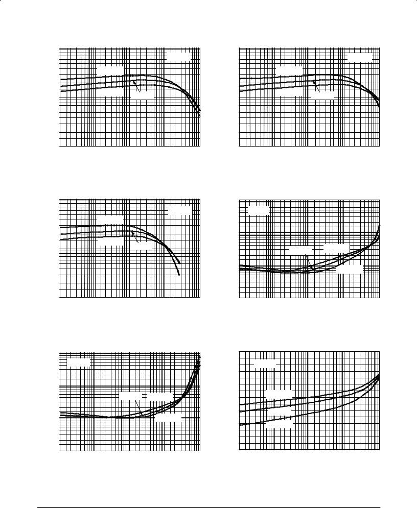
TYPICAL STATIC CHARACTERISTICS
|
100 |
|
|
|
|
|
|
|
|
|
VCE = 1 V |
GAIN |
|
TJ = 125°C |
|
|
|
|
|
|
|
|
|
, DC CURRENT |
10 |
TJ = ± 20°C |
|
TJ = 25°C |
|
|
|
|
|||
|
|
|
|
|
|
FE |
|
|
|
|
|
h |
|
|
|
|
|
|
1 |
|
|
|
|
|
0.001 |
0.01 |
0.1 |
1 |
10 |
|
|
IC, COLLECTOR CURRENT (AMPS) |
|
||
Figure 1. DC Current Gain @ 1 Volt
|
100 |
|
|
|
|
|
|
|
|
|
VCE = 5 V |
GAIN |
|
|
TJ = 125°C |
|
|
|
|
|
|
|
|
, DC CURRENT |
10 |
|
TJ = ± 20°C |
TJ = 25°C |
|
|
|
|
|||
|
|
|
|
|
|
FE |
|
|
|
|
|
h |
|
|
|
|
|
|
1 |
|
|
|
|
|
0.01 |
0.1 |
1 |
10 |
100 |
|
|
IC, COLLECTOR CURRENT (AMPS) |
|
||
Figure 3. DC Current Gain @ 5 Volt
|
10 |
|
|
|
|
|
|
|
IC/IB = 10 |
|
|
|
|
(VOLTS) |
1 |
|
|
|
|
|
|
|
|
|
|
|
|
,VOLTAGE |
|
T |
J |
= 25°C |
° |
|
|
|
|
TJ = ± 20 C |
|
||
0.1 |
|
|
|
TJ = 125°C |
|
|
CE |
|
|
|
|
||
V |
|
|
|
|
|
|
|
0.01 |
0.01 |
|
|
|
|
|
0.001 |
0.1 |
1 |
10 |
||
|
|
IC, COLLECTOR CURRENT (AMPS) |
|
|||
Figure 5. Collector±Emitter Saturation Voltage
|
100 |
|
|
|
|
|
|
|
|
|
VCE = 3 V |
GAIN |
|
TJ = 125°C |
|
|
|
|
|
|
|
|
|
, DC CURRENT |
10 |
TJ = ± 20°C |
|
TJ = 25°C |
|
|
|
|
|||
|
|
|
|
|
|
FE |
|
|
|
|
|
h |
|
|
|
|
|
|
1 |
|
|
|
|
|
0.001 |
0.01 |
0.1 |
1 |
10 |
IC, COLLECTOR CURRENT (AMPS)
Figure 2. DC Current Gain @ 3 Volt
|
10 |
|
|
|
|
|
|
IC/IB = 5 |
|
|
|
(VOLTS) |
1 |
|
|
|
|
|
|
|
|
|
|
,VOLTAGE |
|
|
TJ = 25°C |
TJ = ± 20°C |
|
0.1 |
|
|
|
|
|
CE |
|
|
TJ = 125°C |
|
|
|
|
|
|
||
V |
|
|
|
|
|
|
0.01 |
0.01 |
|
|
|
|
0.001 |
0.1 |
1 |
10 |
|
|
|
IC, COLLECTOR CURRENT (AMPS) |
|
||
Figure 4. Collector±Emitter Saturation Voltage
|
1.5 |
|
|
|
|
|
|
|
|
IC/IB = 5 |
|
|
|
|
|
(VOLTS) |
1 |
|
|
|
|
|
|
|
TJ = ± 20°C |
|
|
|
|||
VOLTAGE |
|
|
|
|
|||
0.5 |
T |
J |
= 25°C |
|
|
|
|
, |
|
|
|
|
|
||
BE |
|
|
|
|
|
|
|
|
TJ = 125°C |
|
|
|
|||
V |
|
|
|
|
|||
|
|
|
|
|
|||
|
0 |
|
|
|
0.1 |
|
|
|
0.001 |
0.01 |
1 |
10 |
|||
|
|
IC, COLLECTOR CURRENT (AMPS) |
|
||||
Figure 6. Base±Emitter Saturation Region
4 |
Motorola Bipolar Power Transistor Device Data |
BUH100
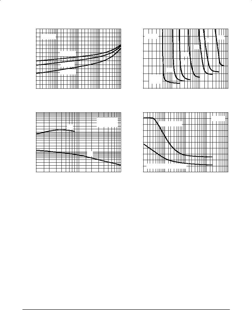
TYPICAL STATIC CHARACTERISTICS
|
1.5 |
|
|
|
|
|
|
IC/IB = 10 |
|
|
|
(VOLTS) |
1 |
|
|
|
|
|
|
TJ = ± 20°C |
|
|
|
VOLTAGE |
|
|
|
|
|
0.5 |
|
TJ = 25°C |
|
|
|
, |
|
|
|
|
|
BE |
|
TJ = 125°C |
|
|
|
|
|
|
|
||
V |
|
|
|
|
|
|
0 |
0.01 |
|
|
|
|
0.001 |
0.1 |
1 |
10 |
IC, COLLECTOR CURRENT (AMPS)
Figure 7. Base±Emitter Saturation Region
|
10000 |
|
|
|
|
TJ = 25°C |
|
|
|
f(test) = 1 MHz |
|
(pF) |
|
Cib |
|
1000 |
|
|
|
CAPACITANCE |
100 |
Cob |
|
C, |
|
||
|
|
||
|
10 |
|
|
|
1 |
10 |
100 |
|
|
VR, REVERSE VOLTAGE (VOLTS) |
|
Figure 9. Capacitance
|
2 |
|
|
|
|
TJ = 25°C |
|
|
15 A |
(VOLTS) |
1.5 |
|
|
10 A |
|
|
|
||
|
|
8 A |
|
|
|
|
|
|
|
VOLTAGE, |
1 |
|
5 A |
|
|
|
|
||
|
|
|
|
|
|
|
|
3 A |
|
CE |
|
2 A |
|
|
V |
0.5 |
|
|
|
|
|
|
|
|
|
VCE(sat) |
|
|
|
|
(IC = 1 A) |
|
|
|
|
0 |
|
|
|
|
0.01 |
0.1 |
1 |
10 |
IB, BASE CURRENT (A)
Figure 8. Collector Saturation Region
|
900 |
|
|
|
|
|
|
|
|
|
TJ = 25°C |
|
800 |
BVCER @ 10 mA |
|
|
|
(VOLTS) |
700 |
|
|
|
|
|
|
|
|
|
|
BVCER |
600 |
|
|
|
|
|
|
|
|
|
|
|
500 |
|
|
|
|
|
|
BVCER(sus) @ 500 mA, 25 mH |
|
|
|
|
400 |
|
1000 |
10000 |
|
|
10 |
100 |
100000 |
||
|
|
|
RBE (Ω) |
|
|
Figure 10. Resistive Breakdown
Motorola Bipolar Power Transistor Device Data |
5 |