Материал: HGTD8P50

HGTD8P50G1, HGTD8P50G1S
Operating Frequency Information |
Handling Precautions for IGBTs |
Operating frequency information for a typical device (Figure 10) is presented as a guide for estimating device performance for a specific application. Other typical frequency vs collector current (ICE) plots are possible using the information shown for a typical unit in Figure 7, Figure 8 and Figure 9. The operating frequency plot (Figure 10) of a typical device shows
fMAX1 or fMAX2 whichever is smaller at each point. The information is based on measurements of a typical device and is
bounded by the maximum rated junction temperature.
fMAX1 is defined by fMAX1 = 0.05/tD(OFF)I. tD(OFF)I deadtime (the denominator) has been arbitrarily held to 10% of the on-
state time for a 50% duty factor. Other definitions are
possible. tD(OFF)I is defined as the time between the 90% point of the trailing edge of the input pulse and the point
where the collector current falls to 90% of its maximum value. Device Turn-Off delay can establish an additional frequency limiting condition for an application other than TJMAX.
tD(OFF)I is important when controlling output ripple under a lightly loaded condition. fMAX2 is defined by fMAX2 = (PD -
PC)/EOFF. The allowable dissipation (PD) is defined by PD = (TJMAX - TC)/RθJC. The sum of device switching and conduction losses must not exceed Pd. A 50% duty factor was used
(Figure 10) and the conduction losses (Pc) are approximated
by Pc = (VCE ∙ ICE)/2. EOFF is defined as the integral of the instantaneous power loss starting at the trailing edge of the
input pulse and ending at the point where the collector current equals zero (ICE = 0A).
The switching power loss (Figure 10) is defined as fMAX2 ∙ EOFF. Turn-On switching losses are not included because
they can be greatly influenced by external circuit conditions and components.
Insulated Gate Bipolar Transistors are susceptible to gateinsulation damage by the electrostatic discharge of energy through the devices. When handling these devices, care should be exercised to assure that the static charge built in the handler’s body capacitance is not discharged through the device. With proper handling and application procedures, however, IGBTs are currently being extensively used in production by numerous equipment manufacturers in military, industrial and consumer applications, with virtually no damage problems due to electrostatic discharge. IGBTs can be handled safely if the following basic precautions are taken:
1.Prior to assembly into a circuit, all leads should be kept shorted together either by the use of metal shorting springs or by the insertion into conductive material such as “† ECCOSORBD LD26” or equivalent.
2.When devices are removed by hand from their carriers, the hand being used should be grounded by any suitable means - for example, with a metallic wristband.
3.Tips of soldering irons should be grounded.
4.Devices should never be inserted into or removed from circuits with power on.
5.Gate Voltage Rating - Never exceed the gate-voltage
rating of VGEM. Exceeding the rated VGE can result in permanent damage to the oxide layer in the gate region.
6.Gate Termination - The gates of these devices are essentially capacitors. Circuits that leave the gate opencircuited or floating should be avoided. These conditions can result in Turn-On of the device due to voltage buildup on the input capacitor due to leakage currents or pickup.
7.Gate Protection - These devices do not have an internal monolithic zener diode from gate to emitter. If gate protection is required an external zener is recommended.
† Trademark Emerson and Cumming, Inc.
HARRIS SEMICONDUCTOR IGBT PRODUCT IS COVERED BY ONE OR MORE OF THE FOLLOWING U.S. PATENTS:
4,364,073 |
4,417,385 |
4,430,792 |
4,443,931 |
4,466,176 |
4,516,143 |
4,532,534 |
4,567,641 |
4,587,713 |
4,598,461 |
4,605,948 |
4,618,872 |
4,620,211 |
4,631,564 |
4,639,754 |
4,639,762 |
4,641,162 |
4,644,637 |
4,682,195 |
4,684,413 |
4,694,313 |
4,717,679 |
4,743,952 |
4,783,690 |
4,794,432 |
4,801,986 |
4,803,533 |
4,809,045 |
4,809,047 |
4,810,665 |
4,823,176 |
4,837,606 |
4,860,080 |
4,883,767 |
4,888,627 |
4,890,143 |
4,901,127 |
4,904,609 |
4,933,740 |
4,963,951 |
4,969,027 |
|
|
|
|
|
|
|
6
HGTD8P50G1, HGTD8P50G1S
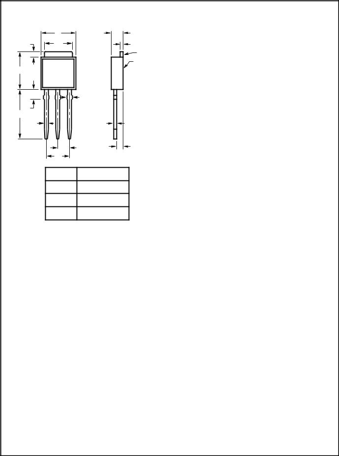
TO-251AA
3 LEAD JEDEC TO-251AA PLASTIC PACKAGE
|
E |
A |
H1 |
b2 |
A1 |
TERM. 4
SEATING
PLANE
D
|
|
b1 |
L1 |
|
|
L |
|
|
b |
|
c |
1 |
2 |
3 |
|
e |
J1 |
|
e1 |
|
Lead 1 |
Gate |
|
Lead 2 |
Collector |
|
Lead 3 |
Emitter |
|
Term. 4 |
Collector |
|
|
INCHES |
MILLIMETERS |
|
||
SYMBOL |
|
|
|
|
NOTES |
MIN |
MAX |
MIN |
MAX |
||
|
|
|
|
|
|
A |
0.086 |
0.094 |
2.19 |
2.38 |
- |
|
|
|
|
|
|
A1 |
0.018 |
0.022 |
0.46 |
0.55 |
3, 4 |
b |
0.028 |
0.032 |
0.72 |
0.81 |
3, 4 |
|
|
|
|
|
|
b1 |
0.033 |
0.040 |
0.84 |
1.01 |
3 |
b2 |
0.205 |
0.215 |
5.21 |
5.46 |
3, 4 |
c |
0.018 |
0.022 |
0.46 |
0.55 |
3, 4 |
|
|
|
|
|
|
D |
0.270 |
0.290 |
6.86 |
7.36 |
- |
|
|
|
|
|
|
E |
0.250 |
0.265 |
6.35 |
6.73 |
- |
|
|
|
|
|
|
e |
0.090 TYP |
2.28 TYP |
5 |
||
|
|
|
|
||
e1 |
0.180 BSC |
4.57 BSC |
5 |
||
H1 |
0.035 |
0.045 |
0.89 |
1.14 |
- |
J1 |
0.040 |
0.045 |
1.02 |
1.14 |
6 |
L |
0.355 |
0.375 |
9.02 |
9.52 |
- |
|
|
|
|
|
|
L1 |
0.075 |
0.090 |
1.91 |
2.28 |
2 |
NOTES:
1.These dimensions are within allowable dimensions of Rev. C of JEDEC TO-251AA outline dated 9-88.
2.Solder finish uncontrolled in this area.
3.Dimension (without solder).
4.Add typically 0.002 inches (0.05mm) for solder plating.
5.Position of lead to be measured 0.250 inches (6.35mm) from bottom of dimension D.
6.Position of lead to be measured 0.100 inches (2.54mm) from bottom of dimension D.
7.Controlling dimension: Inch.
8.Revision 2 dated 10-95.
7
HGTD8P50G1, HGTD8P50G1S
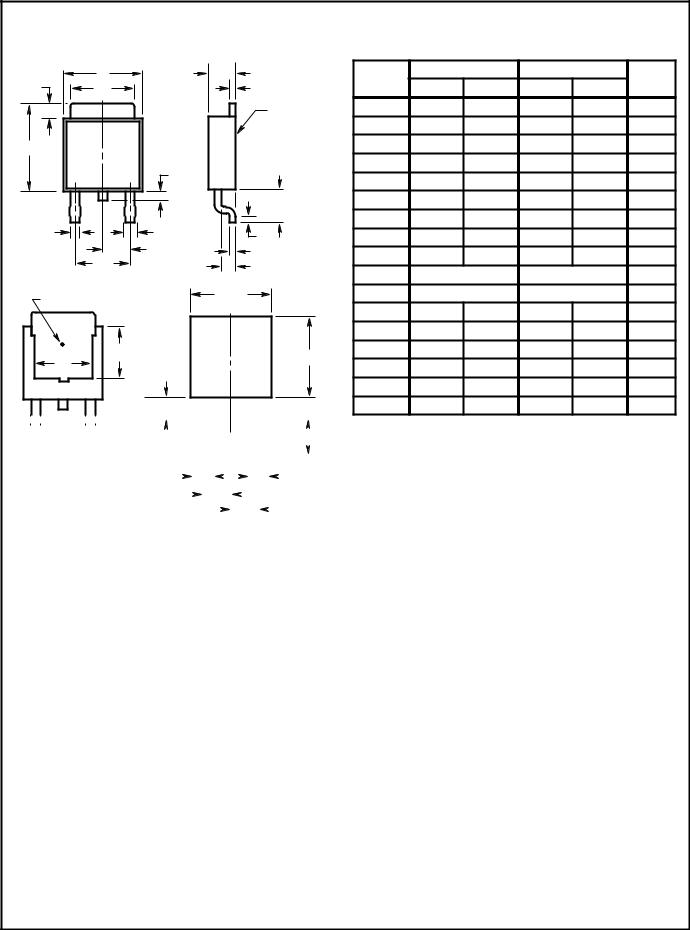
TO-252AA |
|
|
|
|
|
|
|
|
|
SURFACE MOUNT JEDEC TO-252AA PLASTIC PACKAGE |
|
|
|
|
|
|
|||
|
E |
A |
|
INCHES |
MILLIMETERS |
|
|||
|
|
SYMBOL |
MIN |
MAX |
MIN |
MAX |
NOTES |
||
H1 |
b2 |
A1 |
|||||||
|
|
SEATING |
A |
0.086 |
0.094 |
2.19 |
2.38 |
- |
|
|
|
|
|
|
|
|
|
||
|
|
PLANE |
A1 |
0.018 |
0.022 |
0.46 |
0.55 |
4, 5 |
|
|
|
|
|||||||
D |
|
|
b |
0.028 |
0.032 |
0.72 |
0.81 |
4, 5 |
|
|
|
|
|
|
|
|
|
||
|
|
|
b1 |
0.033 |
0.040 |
0.84 |
1.01 |
4 |
|
|
L 2 |
|
b2 |
0.205 |
0.215 |
5.21 |
5.46 |
4, 5 |
|
1 |
3 |
L |
b3 |
0.190 |
- |
4.83 |
- |
2 |
|
c |
0.018 |
0.022 |
0.46 |
0.55 |
4, 5 |
||||
|
|||||||||
|
|
|
|||||||
b |
b1 |
L1 |
D |
0.270 |
0.290 |
6.86 |
7.36 |
- |
|
|
e |
c |
E |
0.250 |
0.265 |
6.35 |
6.73 |
- |
|
|
e1 |
|
|||||||
|
J1 |
e |
0.090 TYP |
2.28 TYP |
7 |
||||
|
|
||||||||
TERM. 4 |
|
0.265 |
e1 |
0.180 BSC |
4.57 BSC |
7 |
|||
|
(6.7) |
H1 |
0.035 |
0.045 |
0.89 |
1.14 |
- |
||
|
|
|
|||||||
|
|
|
J1 |
0.040 |
0.045 |
1.02 |
1.14 |
- |
|
|
L3 |
0.265 (6.7) |
L |
0.100 |
0.115 |
2.54 |
2.92 |
- |
|
b3 |
L1 |
0.020 |
- |
0.51 |
- |
4, 6 |
|||
|
|
||||||||
|
|
|
L2 |
0.025 |
0.040 |
0.64 |
1.01 |
3 |
|
|
0.070 (1.8) |
|
L3 |
0.170 |
- |
4.32 |
- |
2 |
|
|
|
|
|
|
|
|
|
|
|
|
|
|
|
|
|
|
|
|
|
|
|
|
|
|
|
|
|
|
|
|
|
|
|
NOTES: |
|
|
|
|
|
|
|
|
|
|
|
|
|
|
|
|
|
|
|
|
|
|
|
|
|
|
|
|
|
|
|
|
|
|
|
||
|
|
|
|
|
|
|
|
|
|
|
|
|
|
|
|
|
|
|
|
|
|
|
|
|
|
|
|
|
|
|
|
|
|
||
BACK VIEW |
|
|
|
|
|
|
|
|
|
|
|
|
|
|
|
|
|
|
|
|
|
|
|
0.118 (3.0) |
1. |
These dimensions are within allowable dimensions of Rev. B of |
|||||||||
|
|
|
|
|
|
|
|
|
|
|
|
|
|
|
|
|
|
|
|
|
|
|
|
|
|
|
|
|
|
|
JEDEC TO-252AA outline dated 9-88. |
||||
|
|
|
|
|
|
|
|
|
|
|
|
|
|
|
|
|
|
|
|
|
|
|
|
|
|
|
|
|
|
|
|||||
0.063 (1.6) |
|
|
|
|
|
|
|
|
|
|
|
|
|
|
|
|
|
|
|
|
|
|
|
0.063 (1.6) |
2. |
L3 and b3 dimensions establish a minimum mounting surface for |
|||||||||
|
|
|
|
|
|
|
|
|
|
|
|
|
|
|
|
|
|
|
|
|
|
|
|||||||||||||
|
|
|
|
0.090 (2.3) |
|
|
|
|
|
|
|
|
|
|
|
|
|
|
|
|
|
|
|
|
|
|
|
|
|
terminal 4. |
|||||
|
|
|
|
|
|
|
|
|
|
|
|
|
|
|
|
|
|
|
|
|
|
|
0.090 (2.3) |
3. |
Solder finish uncontrolled in this area. |
||||||||||
|
|
|
|
|
|
|
|
|
|
|
|
|
|
|
|
|
|
|
|
|
|
|
|||||||||||||
|
|
|
|
|
|
|
|
|
|
|
|
|
|
|
|
|
|
|
|
|
|
|
|
|
|
|
|
4. |
Dimension (without solder). |
||||||
|
|
|
|
MINIMUM PAD SIZE RECOMMENDED FOR |
|||||||||||||||||||||||||||||||
|
|
|
|
5. Add typically 0.002 inches (0.05mm) for solder plating. |
|||||||||||||||||||||||||||||||
|
|
|
|
|
SURFACE-MOUNTED APPLICATIONS |
6. |
L1 is the terminal length for soldering. |
||||||||||||||||||||||||||||
|
|
|
|
|
|
|
|
|
|
|
|
|
|
|
|
|
|
|
|
|
|
|
|
|
|
|
|
|
|
|
|
|
|
||
|
|
|
|
|
|
|
|
|
|
|
|
|
|
|
|
|
|
|
|
|
|
|
|
|
|
|
|
|
|
|
|
|
|
7. |
Position of lead to be measured 0.090 inches (2.28mm) from bottom |
|
|
|
Lead 1 |
|
|
Gate |
|
|
|
|
|
|
|
|
|
of dimension D. |
|||||||||||||||||||
|
|
|
|
|
|
|
|
|
|
|
|
|
8. |
Controlling dimension: Inch. |
|||||||||||||||||||||
|
|
|
|
|
|
|
|
|
|
|
|
|
|
|
|
|
|
|
|
|
|
|
|
|
|
|
|
|
|
|
|
|
|
||
|
|
|
Lead 3 |
|
|
Source |
|
|
|
|
|
|
|
|
9. Revision 5 dated 10-95. |
||||||||||||||||||||
|
|
|
|
|
|
|
|
|
|
|
|
|
|
|
|
|
|
|
|
|
|
|
|
|
|
|
|
|
|
|
|
|
|
|
|
|
|
|
Term. 4 |
|
|
Collector |
|
|
|
|
|
|
|
|
|
|
|||||||||||||||||||
|
|
|
|
|
|
|
|
|
|
|
|
|
|
|
|
|
|
|
|
|
|
|
|
|
|
|
|
|
|
|
|
|
|
|
|
8
HGTD8P50G1, HGTD8P50G1S
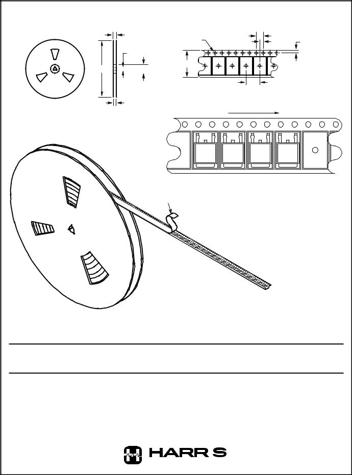
TO-252AA
16mm TAPE AND REEL
22.4mm |
1.5mm |
4.0mm |
|
|
2.0mm |
1.75mm |
|
|
DIA. HOLE |
13mm |
C |
|
L |
16mm
330mm |
|
50mm |
|
|
|||
|
|
|
|
8.0mm
16.4mm
USER DIRECTION OF FEED
GENERAL INFORMATION
COVER TAPE |
1. USE "9A" SUFFIX ON PART NUMBER. |
|
|
|
2. 2500 PIECES PER REEL. |
|
3. ORDER IN MULTIPLES OF FULL REELS ONLY. |
|
4. MEETS EIA-481 REVISION "A" SPECIFICATIONS. |
Revision 5 dated 10-95
All Harris Semiconductor products are manufactured, assembled and tested under ISO9000 quality systems certification.
Harris Semiconductor products are sold by description only. Harris Semiconductor reserves the right to make changes in circuit design and/or specifications at any time without notice. Accordingly, the reader is cautioned to verify that data sheets are current before placing orders. Information furnished by Harris is believed to be accurate and reliable. However, no responsibility is assumed by Harris or its subsidiaries for its use; nor for any infringements of patents or other rights of third parties which may result from its use. No license is granted by implication or otherwise under any patent or patent rights of Harris or its subsidiaries.
Sales Office Headquarters
For general information regarding Harris Semiconductor and its products, call 1-800-4-HARRIS
NORTH AMERICA |
EUROPE |
ASIA |
||
Harris Semiconductor |
Harris Semiconductor |
Harris Semiconductor PTE Ltd. |
||
P. O. Box 883, Mail Stop 53-210 |
Mercure Center |
No. 1 Tannery Road |
||
Melbourne, FL 32902 |
100, Rue de la Fusee |
Cencon 1, #09-01 |
||
TEL: 1-800-442-7747 |
1130 Brussels, Belgium |
Singapore 1334 |
||
(407) 729-4984 |
TEL: (32) 2.724.2111 |
TEL: (65) 748-4200 |
||
FAX: (407) 729-5321 |
FAX: (32) 2.724.22.05 |
FAX: (65) 748-0400 |
||
|
|
|
||
|
|
|
|
|
|
S E M I C O N D U C T O R |
|
||
9