Материал: Library Expert Surface Mount Families
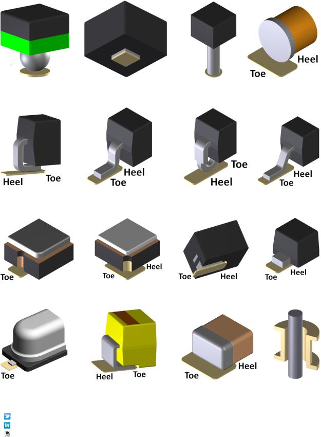
 Library Expert Surface Mount Families
Component Terminal Lead Forms
Ball Grid Array |
Land Grid Array/Bottom Only Column Grid Array |
Cylindrical End Cap |
Inward L Lead |
Outward L Lead |
J Lead |
Gull Wing |
Side Concave |
Corner Concave |
Flat No Lead Side |
Flat Lead |
Under Body Outward L |
Inward Flat Ribbon L |
Rectangular End Cap |
Through Hole |
https://twitter.com/pcblibraries |
© 2014 2019 PCB Libraries, Inc. |
||
https://www.linkedin.com/company/3196824 |
Get updates at www.PCBLibraries.com/downloads |
||
http://www.PCBLibraries.com/forum |
|
updated 10 21 18 |
|

 Library Expert Surface Mount Families
Polarity Marking Legend
The goal of the Polarity Marking Legend is to aid assembly to avoid polarized component packages from being inverted during the assembly machine setup or manual solder process. Therefore, Polarity Marking is only necessary on land patterns that require a specific rotation during the assembly process. For very dense part placements, the polarity marker can be placed under the package and covered up during the assembly process. However, the best practice is to locate the polarity indicator outside the package so that it is visible after the assembly process to allow the end user to visually validate that the assembly insertion process is correct. This is typically known as “Post Assembly Inspection Process”.
Polarity Markings are unique from company to company. Here are samples of the most popular shapes.
The size, rotation and location of the Polarity Markings are user definable. Here are some recommendations.
The most popular polarity marking is a filled Dot. The size of the Polarity Marking is relevant to the size of the component package and pad width. However, the polarity dot size is also dependent on the part placement density and the assembly shops ability to easily locate the dot to avoid component rotation insertion errors. The smallest visible markings range from 0.25 mm – 0.40 mm and are typically used for micro miniature packages or very dense part placement PCB layouts. The average size ranges are 0.50 mm – 0.80 mm. The largest recommended polarity dot is 1.00 mm.
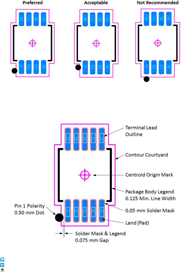
This illustration indicates 3 popular locations for a 0.50 mm dot on an SOP package. The preferred polarity dot placement is at the end of the pad which is the furthest distance from the component package body. This makes the post assembly inspection process easy as the component package may move up ordown during assembly reflow but the dot will always be visible. The acceptable location is the pad center but this location is also a potential via site. It is advisable to keep legend ink off non tented vias or tented via holes. The not recommended location has a higher potential of a via site and the marking could collide with other parts during the part placement process.
https://twitter.com/pcblibraries |
© 2014 2019 PCB Libraries, Inc. |
https://www.linkedin.com/company/3196824 |
Get updates at www.PCBLibraries.com/downloads |
http://www.PCBLibraries.com/forum |
updated 10 21 18 |
 Library Expert Surface Mount Families
Gull Wing Terminal Lead Legend Polarity Marking Location
The component body outline legend line width should be a minimum of 0.125 mm. The Polarity Marking Symbol and component body legend should have a minimum 0.075 mm gap from the solder mask. The figure below illustrates the anatomy of a land pattern and feature sizes and spaces.
Sample 0.50 mm Pitch SOP Legend and Polarity Marking Rules
https://twitter.com/pcblibraries |
© 2014 2019 PCB Libraries, Inc. |
https://www.linkedin.com/company/3196824 |
Get updates at www.PCBLibraries.com/downloads |
http://www.PCBLibraries.com/forum |
updated 10 21 18 |
 Library Expert Surface Mount Families
Warning, check with your PCB manufacturer to verify if they can meet the dimensional requirements.
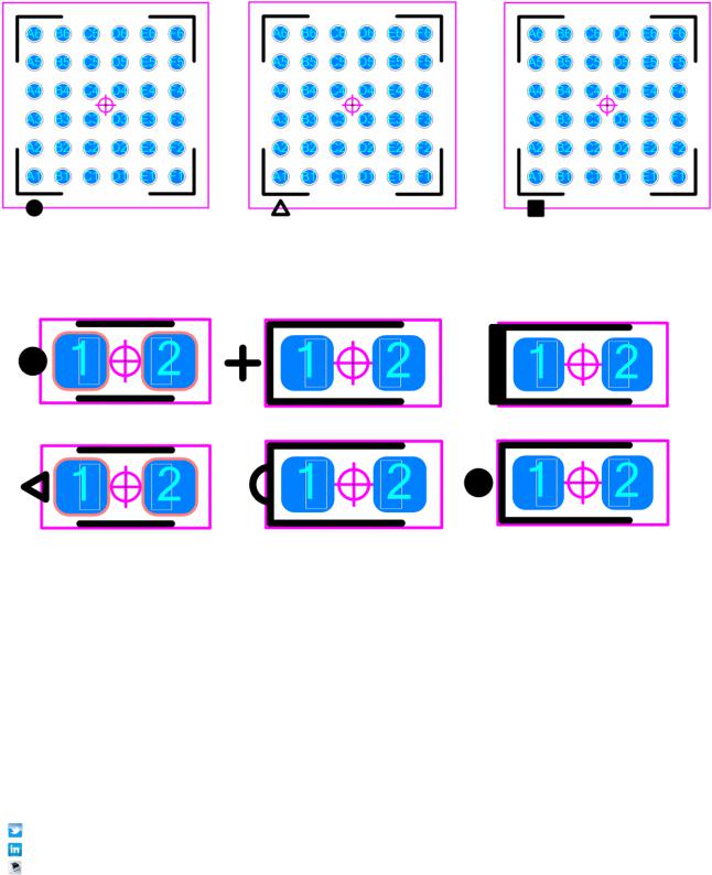
Bottom only termination packages – BGA, LGA, CGA, QFN, PQFN, SON, PSON and DFN
The polarity marking size should match the Terminal Width. The gap between the body legend and the polarity marker should range from 0.15 mm – 0.25 mm
Polarized chip capacitors packages.
https://twitter.com/pcblibraries |
© 2014 2019 PCB Libraries, Inc. |
https://www.linkedin.com/company/3196824 |
Get updates at www.PCBLibraries.com/downloads |
http://www.PCBLibraries.com/forum |
updated 10 21 18 |