Материал: MJ10007R
MOTOROLA
SEMICONDUCTOR TECHNICAL DATA
Order this document by MJ10007/D
Designer's Data Sheet
SWITCHMODE Series
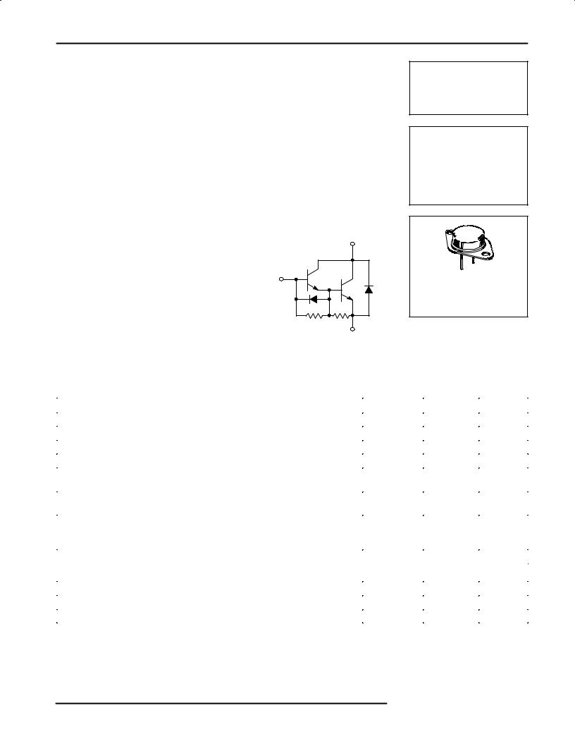
NPN Silicon Power Darlington Transistors with Base-Emitter Speedup Diode
The MJ10007 Darlington transistor is designed for high±voltage, high±speed, power switching in inductive circuits where fall time is critical. It is particularly suited for line operated switchmode applications such as:
•Switching Regulators
•Inverters
•Solenoid and Relay Drivers
• Motor Controls
• Deflection Circuits
Fast Turn±Off Times
30 ns Inductive Fall Time Ð 25 _C (Typ) |
|
|
500 ns Inductive Storage Time Ð 25 _C (Typ) |
|
|
Operating Temperature Range ±65 to +200_C |
|
|
100_C Performance Specified for: |
≈ 100 |
≈ 15 |
|
|
MJ10007*
*Motorola Preferred Device
10 AMPERE
NPN SILICON
POWER DARLINGTON
TRANSISTORS
400 VOLTS
150 WATTS
CASE 1±07 TO±204AA (TO±3)
Reversed Biased SOA with Inductive Loads
Switching Times with Inductive Loads
Saturation Voltages
Leakage Currents
MAXIMUM RATINGS
Rating |
Symbol |
Value |
Unit |
|
|
|
|
Collector±Emitter Voltage |
VCEO |
400 |
Vdc |
Collector±Emitter Voltage |
VCEX |
450 |
Vdc |
Collector±Emitter Voltage |
VCEV |
500 |
Vdc |
Emitter Base Voltage |
VEB |
8.0 |
Vdc |
Collector Current Ð Continuous |
IC |
10 |
Adc |
Ð Peak (1) |
ICM |
20 |
|
Base Current Ð Continuous |
IB |
2.5 |
Adc |
Ð Peak (1) |
IBM |
5.0 |
|
Total Power Dissipation @ TC = 25_C |
PD |
150 |
Watts |
@ TC = 100_C |
|
100 |
|
Derate above 25_C |
|
0.86 |
_ |
|
|
|
W/ C |
Operating and Storage Junction Temperature Range |
TJ, Tstg |
± 65 to +200 |
_C |
THERMAL CHARACTERISTICS
Characteristic |
Symbol |
Max |
Unit |
|
|
|
|
Thermal Resistance, Junction to Case |
RqJC |
1.17 |
_C/W |
Maximum Lead Temperature for Soldering Purposes 1/8″ from Case for 5 Seconds |
TL |
275 |
_C |
(1) Pulse Test: Pulse Width = 5.0 ms, Duty Cycle v 10%.
Designer's and SWITCHMODE are trademarks of Motorola, Inc.
Designer's Data for ªWorst Caseº Conditions Ð The Designer 's Data Sheet permits the design of most circuits entirely from the information presented. SOA Limit curves Ð representing boundaries on device characteristics Ð are given to facilitate ªworst caseº design.
Preferred devices are Motorola recommended choices for future use and best overall value.
REV 2
Motorola, Inc. 1995

MJ10007
ELECTRICAL CHARACTERISTICS (TC = 25_C unless otherwise noted)
|
|
Characteristic |
Symbol |
Min |
Typ |
Max |
Unit |
|
|
|
|
|
|
|
|
OFF CHARACTERISTICS |
|
|
|
|
|
||
|
|
|
|
|
|
|
|
Collector±Emitter Sustaining Voltage (Table 1) |
VCEO(sus) |
400 |
Ð |
Ð |
Vdc |
||
(IC = 250 mA, IB = 0, Vclamp = Rated VCEO) |
|
|
|
|
|
||
Collector±Emitter Sustaining Voltage (Table 1, Figure 12) |
VCEX(sus) |
450 |
|
|
Vdc |
||
(IC = 1 A, Vclamp = Rated VCEX, TC = 100_C) |
|
Ð |
Ð |
|
|||
(IC = 5 A, Vclamp = Rated VCEX, TC = 100_C) |
|
325 |
Ð |
Ð |
|
||
Collector Cutoff Current |
ICEV |
|
|
|
mAdc |
||
(VCEV = Rated Value, VBE(off) = 1 5 Vdc) |
|
Ð |
Ð |
0.25 |
|
||
(VCEV = Rated Value, VBE(off) = 1.5 Vdc, TC = 150_C) |
|
Ð |
Ð |
5.0 |
|
||
Collector Cutoff Current |
ICER |
Ð |
Ð |
5.0 |
mAdc |
||
(VCE = Rated VCEV, RBE = 50 Ω, TC = 100_C) |
|
|
|
|
|
||
Emitter Cutoff Current |
IEBO |
Ð |
Ð |
175 |
mAdc |
||
(VEB = 2 Vdc, IC = 0) |
|
|
|
|
|
||
SECOND BREAKDOWN |
|
|
|
|
|
||
|
|
|
|
|
|
||
Second Breakdown Collector Current with base forward biased |
IS/b |
|
See Figure 11 |
|
|||
ON CHARACTERISTICS (2) |
|
|
|
|
|
||
|
|
|
|
|
|
|
|
DC Current Gain |
|
hFE |
|
|
|
Ð |
|
(IC = 2.5 Adc, VCE = 5.0 Vdc) |
|
40 |
Ð |
500 |
|
||
(IC = 5.0 Adc, VCE = 5.0 Vdc) |
|
30 |
Ð |
300 |
|
||
Collector Emitter Saturation Voltage |
VCE(sat) |
|
|
|
Vdc |
||
(IC = 5.0 Adc, IB = 250 mAdc) |
|
Ð |
Ð |
1.9 |
|
||
(IC = 10 Adc, IB = 1.0 Adc) |
|
Ð |
Ð |
2.9 |
|
||
(IC = 5.0 Adc, IB = 250 mAdc, TC = 100_C) |
|
Ð |
Ð |
2.0 |
|
||
Base±Emitter Saturation Voltage |
VBE(sat) |
|
|
|
Vdc |
||
(IC = 5.0 Adc, IB = 250 mAdc) |
|
Ð |
Ð |
2.5 |
|
||
(IC = 5.0 Adc, IB = 250 mAdc, TC = 100_C) |
|
Ð |
Ð |
2.5 |
|
||
Diode Forward Voltage (1) |
Vf |
Ð |
3.0 |
5 |
Vdc |
||
(IF = 5.0 Adc) |
|
|
|
|
|
|
|
DYNAMIC CHARACTERISTICS |
|
|
|
|
|
||
|
|
|
|
|
|
|
|
Small Signal Current Gain |
hfe |
10 |
Ð |
Ð |
Ð |
||
(IC = 1.0 Adc, VCE = 10 Vdc, ftest = 1.0 MHz) |
|
|
|
|
|
||
Output Capacitance |
|
Cob |
60 |
Ð |
275 |
pF |
|
(VCB = 10 Vdc, IE = 0, ftest = 100 kHz) |
|
|
|
|
|
||
SWITCHING CHARACTERISTICS |
|
|
|
|
|
||
|
|
|
|
|
|
|
|
Resistive Load (Table 1) |
|
|
|
|
|
||
|
|
|
|
|
|
|
|
Delay Time |
|
|
td |
Ð |
0.05 |
0.2 |
μs |
Rise Time |
|
(VCC = 250 Vdc, IC = 5.0 A, |
t |
Ð |
0.25 |
0.6 |
μs |
|
|
IB1 = 250 mA, VBE(off) = 5.0 Vdc, tp = 50 μs, |
r |
|
|
|
|
Storage Time |
|
ts |
Ð |
0.5 |
1.5 |
μs |
|
|
Duty Cycle v 2.0%) |
||||||
Fall Time |
|
|
tf |
Ð |
0.06 |
0.5 |
μs |
Inductive Load Clamped (Table 1) |
|
|
|
|
|
||
|
|
|
|
|
|
|
|
Storage Time |
|
(IC = 5.0 A(pk), Vclamp = Rated VCEX, IB1 = 250 mA, |
tsv |
Ð |
0.8 |
2.0 |
μs |
Crossover Time |
|
VBE(off) = 5.0 Vdc, TC = 100_C) |
t |
Ð |
0.6 |
1.5 |
μs |
|
|
|
c |
|
|
|
|
Storage Time |
|
(IC = 5.0 A(pk), Vclamp = Rated VCEX, IB1 = 250 mA, |
tsv |
Ð |
0.5 |
Ð |
μs |
Crossover Time |
|
VBE(off) = 5.0 Vdc, TC = 25_C) |
t |
Ð |
0.3 |
Ð |
μs |
|
|
|
c |
|
|
|
|
(1) The internal Collector±to±Emitter diode can eliminate the need for an external diode to clamp inductive loads.
(1)Tests have shown that the Forward Recovery Voltage (Vf) of this diode is comparable to that of typical fast recovery rectifiers.
(2)Pulse Test: PW = 300 μs, Duty Cycle v 2%.
2 |
Motorola Bipolar Power Transistor Device Data |
hFE, DC CURRENT GAIN
|
|
|
|
|
|
|
|
|
|
|
|
|
|
|
|
|
|
|
|
|
|
|
|
|
|
|
|
|
|
|
|
|
|
|
|
|
|
|
|
MJ10007 |
|||||||
|
|
|
|
|
|
|
|
|
|
|
|
|
|
|
TYPICAL CHARACTERISTICS |
|
|
|
|
|
|
|
|
|
|
|
|
|
|
|
|
|
|
|
|||||||||||||
300 |
|
|
|
|
|
|
|
|
|
|
|
|
|
|
|
|
|
|
|
|
|
|
(VOLTS) |
3 |
|
|
|
|
|
|
|
|
|
|
|
|
|
|
TJ = 25°C |
|
|
||||||
|
|
|
|
|
|
|
|
|
|
|
|
|
|
|
|
|
|
|
|
|
|
|
3.4 |
|
|
|
|
|
|
|
|
|
|
|
|
|
|
|
|
|
|
|
|
|
|
|
|
200 |
|
|
|
|
|
|
|
T |
J |
= |
150 |
°C |
|
|
|
|
|
|
|
|
|
|
VOLTAGE |
|
|
|
|
|
|
|
|
|
|
|
|
|
|
|
|
|
|
|
|
|
|
|
|
|
|
|
|
|
|
|
|
|
|
|
|
|
|
|
|
|
|
|
|
|
|
|
|
|
|
|
|
|
|
|
|
|
|
|
|
|
|
|
|
|
|
|
|
|
|
||
100 |
|
|
|
|
|
|
|
|
|
|
|
|
|
|
|
|
|
|
|
|
|
|
|
|
|
|
|
|
|
|
|
|
|
|
|
|
|
|
|
|
|
|
|
|
|
||
|
|
|
|
|
|
|
|
|
|
|
|
|
|
|
|
|
|
|
|
|
|
|
|
|
|
|
|
|
|
|
|
|
|
|
|
|
|
|
|
|
|
|
|
|
|
||
|
|
|
|
|
|
|
|
|
|
|
|
|
|
|
|
|
|
|
|
|
|
IC |
= 0.3 A |
2.5 |
A |
|
|
|
5 |
A |
|
|
|
10 A |
|
|
|
|
|
|
|
||||||
|
|
|
|
|
|
|
|
|
|
|
|
|
|
|
|
|
|
|
|
|
|
|
|
|
|
|
|
|
|
|
|
|
|
|
|
|
|
|
|
|
|
|
|
|
|
|
|
|
|
|
|
|
|
|
|
|
|
|
|
|
|
|
|
|
|
|
|
|
|
|
|
|
|
|
|
|
|
|
|
|
|
|
|
|
|
|
|
|
|
|
|
|
|
|
|
70 |
|
|
|
|
|
|
|
|
|
|
25 |
°C |
|
|
|
|
|
|
|
|
|
|
|
2.6 |
|
|
|
|
|
|
|
|
|
|
|
|
|
|
|
|
|
|
|
|
|
|
|
|
|
|
|
|
|
|
|
|
|
|
|
|
|
|
|
|
|
|
|
|
|
|
|
|
|
|
|
|
|
|
|
|
|
|
|
|
|
|
|
|
|
|
|
||||
|
|
|
|
|
|
|
|
|
|
|
|
|
|
|
|
|
|
|
|
|
|
|
|
|
|
|
|
|
|
|
|
|
|
|
|
|
|
|
|
|
|
|
|
|
|
|
|
50 |
|
|
|
|
|
|
|
|
|
|
|
|
|
|
|
|
|
|
|
|
|
|
COLLECTOR±EMITTER |
1 |
|
|
|
|
|
|
|
|
|
|
|
|
|
|
|
|
|
|
|
|
|
|
|
|
|
|
|
|
|
|
|
|
|
|
|
|
|
|
|
|
|
|
|
|
|
|
|
|
|
|
|
|
|
|
|
|
|
|
|
|
|
|
|
|
|
|
|
|
|||
|
|
|
|
|
|
|
|
|
|
|
|
|
|
|
|
|
|
|
|
|
|
|
|
|
|
|
|
|
|
|
|
|
|
|
|
|
|
|
|
|
|
|
|
|
|||
30 |
|
|
|
|
|
|
|
|
|
|
|
|
|
|
|
|
|
|
|
|
|
|
|
2.2 |
|
|
|
|
|
|
|
|
|
|
|
|
|
|
|
|
|
|
|
|
|
|
|
|
|
|
|
|
|
|
|
|
|
|
|
|
|
|
|
|
|
|
|
|
|
|
|
|
|
|
|
|
|
|
|
|
|
|
|
|
|
|
|
|
|
|
|
|
|
||
|
|
|
|
|
|
|
|
|
|
|
|
|
|
|
|
|
|
|
|
|
|
|
|
|
|
|
|
|
|
|
|
|
|
|
|
|
|
|
|
|
|
|
|
|
|
|
|
|
|
|
|
|
|
|
|
|
± 55 |
°C |
|
|
|
|
|
|
|
|
|
|
|
1.8 |
|
|
|
|
|
|
|
|
|
|
|
|
|
|
|
|
|
|
|
|
|
|
|
||
20 |
|
|
|
|
|
|
|
|
|
|
|
|
|
|
|
|
|
|
|
|
|
|
|
|
|
|
|
|
|
|
|
|
|
|
|
|
|
|
|
|
|
|
|
||||
|
|
|
|
|
|
|
|
|
|
|
|
|
|
|
|
|
|
|
|
|
|
|
|
|
|
|
|
|
|
|
|
|
|
|
|
|
|
|
|
|
|||||||
|
|
|
|
|
|
|
|
|
|
|
|
|
|
|
|
|
|
|
|
|
|
|
|
|
|
|
|
|
|
|
|
|
|
|
|
|
|
|
|
|
|
|
|
|
|
||
10 |
|
|
|
|
|
|
|
|
|
|
|
|
|
|
|
|
|
|
|
|
|
|
|
1.4 |
|
|
|
|
|
|
|
|
|
|
|
|
|
|
|
|
|
|
|
|
|
|
|
|
|
|
|
|
|
|
|
|
|
|
|
|
|
|
|
|
|
|
|
|
|
|
|
|
|
|
|
|
|
|
|
|
|
|
|
|
|
|
|
|
|
|
|
|
|
||
|
|
|
|
|
|
|
|
|
|
|
|
|
|
|
|
|
|
|
|
|
|
|
|
|
|
|
|
|
|
|
|
|
|
|
|
|
|
|
|
|
|
|
|
|
|
||
|
|
|
|
|
|
|
|
|
|
|
|
|
|
|
|
|
|
|
|
|
|
|
|
|
|
|
|
|
|
|
|
|
|
|
|
|
|
|
|
|
|
|
|
|
|
|
|
|
|
|
|
|
|
|
|
|
|
|
|
|
|
|
|
|
|
|
|
|
|
|
|
|
|
|
|
|
|
|
|
|
|
|
|
|
|
|
|
|
|
|
|
|
|
|
|
7 |
|
|
|
|
|
|
|
|
|
|
|
|
|
|
|
|
|
|
|
|
|
|
|
|
|
|
|
|
|
|
|
|
|
|
|
|
|
|
|
|
|
|
|
|
|
|
|
|
|
|
|
|
|
|
|
|
|
|
|
|
|
|
|
|
|
|
|
|
|
|
|
|
|
|
|
|
|
|
|
|
|
|
|
|
|
|
|
|
|
|
|
|
|
|
|
5 |
|
|
|
|
|
|
|
|
|
|
|
|
|
|
|
|
|
|
|
|
|
|
|
|
|
|
|
|
|
|
|
|
|
|
|
|
|
|
|
|
|
|
|
|
|
|
|
|
|
|
|
|
|
|
|
|
|
|
|
|
|
|
|
|
|
|
|
|
|
|
|
|
|
|
|
|
|
|
|
|
|
|
|
|
|
|
|
|
|
|
|
|
|
||
|
|
|
|
|
|
|
|
|
|
|
|
VCE = |
5 V |
|
|
|
|
|
|
|
|
, |
|
|
|
|
|
|
|
|
|
|
|
|
|
|
|
|
|
|
|
|
|
|
|
|
|
|
|
|
|
|
|
|
|
|
|
|
|
|
|
|
|
|
|
|
|
|
CE |
|
|
|
|
|
|
|
|
|
|
|
|
|
|
|
|
|
|
|
|
|
|
|
|
||
|
|
|
|
|
|
|
|
|
|
|
|
|
|
|
|
|
|
|
|
|
|
|
|
|
|
|
|
|
|
|
|
|
|
|
|
|
|
|
|
|
|
|
|
|
|||
|
|
|
|
|
|
|
|
|
|
|
|
|
|
|
|
|
|
|
|
|
|
|
|
|
|
|
|
|
|
|
|
|
|
|
|
|
|
|
|
|
|
|
|
|
|
|
|
3 |
|
|
|
|
|
|
|
|
|
|
|
|
|
|
|
|
|
|
|
|
|
|
V |
0.6 |
|
|
|
|
|
|
|
|
|
|
|
|
|
|
|
|
|
|
|
|
|
|
|
|
|
|
|
|
|
|
|
|
|
|
|
|
|
|
|
|
|
|
|
|
|
|
|
|
|
|
|
|
|
|
|
|
|
|
|
|
|
|
|
|
|
|
|
|
|||
0.1 |
0.2 |
0.3 |
0.5 |
0.7 |
1 |
2 |
3 |
5 |
7 |
10 |
10 |
20 |
30 |
50 |
70 |
100 |
200 |
300 |
500 700 |
|
1 k |
||||||||||||||||||||||||||
|
|
|
|
|
IC, COLLECTOR CURRENT (AMP) |
|
|
|
|
|
|
|
|
|
|
|
|
|
IB, BASE CURRENT (mA) |
|
|
|
|
|
|
|
|
|
|
||||||||||||||||||
|
|
|
|
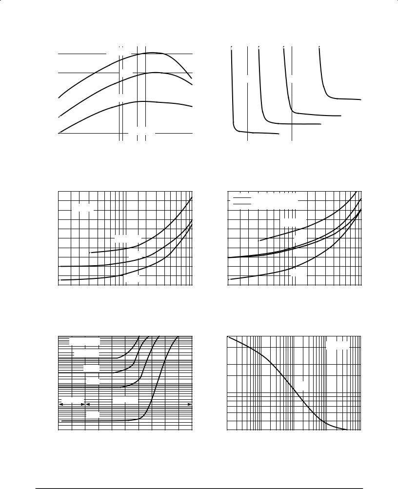
Figure 1. DC Current Gain |
|
|
|
|
|
|
|
|
|
|
|
Figure 2. Collector Saturation Region |
|
|
|||||||||||||||||||||||||||||
COLLECTOR±EMITTER SATURATION |
VOLTAGE (VOLTS) |
, |
|
CE(sat) |
|
V |
|
2.4 |
|
|
|
|
|
|
|
|
|
|
2.8 |
|
|
|
|
|
|
|
|
|
|
|
|
|
|
|
|
|
|
|
|
|
(VOLTS) |
|
|
VBE(sat) @ IC/IB = 10 |
|
|
|
|
|
||||
2 |
IC/IB = 10 |
|
|
|
|
|
|
|
2.4 |
|
VBE(on) @ VCE = 5 V |
|
|
|
|
|
||||||
|
|
|
|
|
|
|
|
|
|
|
|
|
|
|||||||||
|
|
|
|
|
|
|
VOLTAGE |
|
|
|
|
|
|
|
|
|
|
|||||
1.6 |
|
|
|
|
|
|
|
|
|
2 |
|
|
|
TJ = ± 55°C |
|
|
|
|
|
|||
|
|
|
|
|
|
|
|
|
|
|
|
|
|
|
|
|
|
|||||
|
|
|
|
|
|
|
|
|
BASE±EMITTER |
|
|
|
|
|
|
|
|
|
|
|||
0.8 |
|
|
|
TJ = ± 55°C |
|
|
|
|
1.2 |
|
|
|
|
25°C |
|
|
|
|
|
|||
|
|
|
|
|
|
|
|
|
|
|
|
|
|
|
|
|
|
|
||||
1.2 |
|
|
|
|
|
|
|
|
|
|
1.6 |
|
|
|
|
25°C |
|
|
|
|
|
|
|
|
|
|
|
25°C |
|
|
|
|
|
|
|
|
|
|
|
|
|
|
|
||
|
|
|
|
|
|
|
|
|
|
|
|
|
|
|
|
|
|
|
|
|
||
|
|
|
|
|
|
|
|
|
|
, |
|
|
|
|
|
150°C |
|
|
|
|
|
|
|
|
|
|
|
|
|
|
|
|
BE |
|
|
|
|
|
|
|
|
|
|
||
|
|
|
|
|
150°C |
|
|
|
|
V |
|
|
|
|
|
|
|
|
|
|
|
|
0.4 |
|
|
|
|
|
|
|
|
|
0.8 |
|
|
|
|
|
|
|
|
|
|
||
0.2 |
0.3 |
0.5 |
0.7 |
1 |
2 |
3 |
5 |
7 |
10 |
0.2 |
0.3 |
0.5 |
0.7 |
1 |
2 |
3 |
5 |
7 |
10 |
|||
0.1 |
0.1 |
|||||||||||||||||||||
|
|
IC, COLLECTOR CURRENT (AMP) |
|
|
|
|
|
IC, COLLECTOR CURRENT (AMP) |
|
|
|
|||||||||||
Figure 3. Collector-Emitter Saturation Voltage |
Figure 4. Base-Emitter Voltage |
|
103 |
|
|
|
|
|
400 |
|
|
|
|
|
|
|
|
|
|
|
|
VCE |
= 250 V |
|
|
|
|
|
|
|
|
|
|
|
|
|
TJ = 25°C |
|
|
μA) |
|
|
|
|
|
(pF) |
|
|
|
|
|
|
|
|
|
|
||
TJ = 125°C |
|
|
|
|
|
|
|
|
|
|
|
|
|
|
|
|||
CURRENTCOLLECTOR( |
102 |
|
|
|
|
CAPACITANCEOUTPUT, |
200 |
|
|
|
|
|
|
|
|
|
|
|
100 |
100°C |
|
|
|
|
|
|
|
|
|
|
|
|
|
|
|||
|
|
|
|
|
|
|
|
|
|
|
|
|
|
|
|
|
||
|
|
|
|
|
|
|
|
|
|
|
|
|
|
|
|
|
|
|
|
1 |
° |
|
|
|
|
|
|
|
|
|
|
|
|
|
|
|
|
|
10 |
75 C |
|
|
|
|
|
|
|
|
|
|
|
Cob |
|
|
|
|
|
|
|
|
|
|
|
|
|
|
|
|
|
|
|
|
|
|
|
|
|
|
|
|
|
|
100 |
|
|
|
|
|
|
|
|
|
|
|
|
REVERSE |
|
|
FORWARD |
|
|
80 |
|
|
|
|
|
|
|
|
|
|
|
C |
|
|
|
|
|
ob |
|
|
|
|
|
|
|
|
|
|
|
|
, |
|
|
|
|
|
C |
60 |
|
|
|
|
|
|
|
|
|
|
|
I |
|
25°C |
|
|
|
|
|
|
|
|
|
|
|
|
|
|
||
|
|
|
|
|
|
|
|
|
|
|
|
|
|
|
|
|
|
|
|
10±1 |
0 |
+ 0.2 |
+ 0.4 |
+ 0.6 |
+ 0.8 |
40 |
0.2 |
0.5 |
1 |
2 |
5 |
10 |
20 |
50 |
100 200 |
500 |
1000 |
|
± 0.2 |
0.1 |
||||||||||||||||
|
|
VBE, BASE±EMITTER VOLTAGE (VOLTS) |
|
|
|
|
VR, REVERSE VOLTAGE (VOLTS) |
|
|
|||||||||
Figure 5. Collector Cutoff Region |
Figure 6. Output Capacitance |
Motorola Bipolar Power Transistor Device Data |
3 |
MJ10007
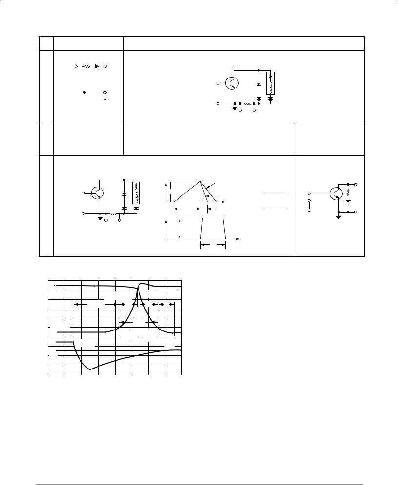
Table 1. Test Conditions for Dynamic Performance
|
|
|
VCEO(sus) |
||||||||||||
|
|
|
|
|
|
|
|
|
|
|
|
|
1 |
||
INPUT CONDITIONS |
20 |
|
|
|
|
|
|
|
|
||||||
0 |
|
|
|
|
|
|
|
|
|
|
|
|
2 |
||
|
|
|
|
|
|
|
|
|
|
|
|
||||
|
|
|
|
|
|
|
|
|
|
|
|
|
|||
|
|
|
|
|
|
||||||||||
|
|
|
|
|
|
|
|||||||||
|
|
|
|
||||||||||||
|
PW Varied to Attain |
||||||||||||||
|
IC = 250 mA |
||||||||||||||
CIRCUIT VALUES |
Lcoil = 10 mH, VCC = 10 V |
||||||||||||||
|
Rcoil = 0.7 Ω |
||||||||||||||
|
Vclamp = VCEO(sus) |
||||||||||||||
INDUCTIVE TEST CIRCUIT
CIRCUITS |
TUT |
|
Rcoil |
|
1 |
1N4937 |
|||
|
|
|||
INPUT |
OR |
Lcoil |
||
EQUIVALENT |
||||
SEE ABOVE FOR |
Vclamp |
|
||
DETAILED CONDITIONS |
V |
|||
|
||||
TEST |
|
|
CC |
|
2 |
RS = |
|
||
|
|
0.1 Ω |
|
VCEX(sus) AND INDUCTIVE SWITCHING |
RESISTIVE SWITCHING |
|
|
INDUCTIVE TEST CIRCUIT
TUT |
|
Rcoil |
|
1 |
1N4937 |
||
INPUT |
OR |
Lcoil |
|
EQUIVALENT |
|||
SEE ABOVE FOR |
|
||
Vclamp |
|
||
DETAILED CONDITIONS |
V |
||
|
|
CC |
|
2 |
RS = |
|
|
|
0.1 Ω |
|
Lcoil = 180 μH |
VCC = 250 V |
|
Rcoil = 0.05 Ω |
||
RL = 50 Ω |
||
Vclamp = Rated VCEX Value |
||
VCC = 20 V |
Pulse Width = 50 μs |
|
fo = 500 kHz |
||
|
OUTPUT WAVEFORMS |
|
|
|
|
|
|
RESISTIVE TEST CIRCUIT |
||
IC |
tf UNCLAMPED [ t2 |
t1 Adjusted to |
|
|
|
||||
Obtain I |
|
|
|
|
|||||
|
|
|
|
|
C |
|
|
|
TUT |
|
|
|
|
Lcoil (ICpk) |
|
||||
IC(pk) |
|
t |
≈ |
1 |
RL |
||||
|
tf CLAMPED |
1 |
|
|
VCC |
|
|
|
|
|
|
|
|
|
2 |
|
|||
|
t |
|
|
L |
|
(I |
) |
VCC |
|
|
|
|
coil |
|
|||||
t1 |
tf |
t2 |
≈ |
|
Cpk |
|
|
|
|
|
VClamp |
|
|
|
|||||
|
|
|
|
|
|
|
|
||
VCE |
|
Test Equipment |
|
|
|||||
VCE or |
|
Scope Ð Tektronix |
|
|
|||||
|
475 or Equivalent |
|
|
||||||
Vclamp |
|
|
|
||||||
TIME |
t |
|
|
|
|
|
|
|
|
t2 |
|
|
|
|
|
|
|
|
|
|
|
|
|
|
|
|
|
|
|
IC |
|
|
V |
|
90% Vclamp |
90% IC |
clamp |
|
|
||
tsv |
trv |
tfi |
tti |
Vclamp |
|
tc |
|
10% |
10% |
|
|
90% IB1 |
Vclamp |
IC |
2% |
|
|
I |
|
|
|
|
C |
IB |
|
|
|
|
TIME |
|
|
Figure 7. Inductive Switching Measurements
SWITCHING TIMES NOTE
In resistive switching circuits, rise, fall, and storage times have been defined and apply to both current and voltage waveforms since they are in phase. However, for inductive loads which are common to SWITCHMODE power supplies and hammer drivers, current and voltage waveforms are not in phase. Therefore, separate measurements must be made on each waveform to determine the total switching time. For this reason, the following new terms have been defined.
tsv = Voltage Storage Time, 90% IB1 to 10% Vclamp trv = Voltage Rise Time, 10±90% Vclamp
tfi = Current Fall Time, 90±10% IC tti = Current Tail, 10±2% IC
tc = Crossover Time, 10% Vclamp to 10% IC
An enlarged portion of the turn±off waveforms is shown in Figure 7 to aid in the visual identity of these terms.
4 |
Motorola Bipolar Power Transistor Device Data |
SWITCHING TIMES NOTE (continued)
For the designer, there is minimal switching loss during storage time and the predominant switching power losses occur during the crossover interval and can be obtained using the standard equation from AN±222.
PSWT = 1/2 VCC IC (tc) f
MJ10007
In general, trv + tfi ]tc. However, at lower test currents this relationship may not be valid.
As is common with most switching transistors, resistive switching is specified at 25_C and has become a benchmark for designers. However, for designers of high frequency converter circuits, the user oriented specifications which make this a ªSWITCHMODEº transistor are the inductive switching speeds (tc and tsv) which are guaranteed at 100_C.
RESISTIVE SWITCHING PERFORMANCE
t, TIME ( μs)
1
0.7VCC = 250 V
0.5 |
|
IB1 = 250 mA |
|
|
|
|
|
|
|
|
|
|
0.3 |
|
TJ = 25°C |
|
|
|
|
|
|
|
|
|
|
|
|
|
|
|
|
|
|
|
|
|
|
|
0.2 |
|
|
|
|
|
|
|
|
|
|
|
|
|
|
|
|
|
|
|
|
|
|
|
|
|
|
|
|
|
|
|
|
|
|
|
|
|
|
0.1 |
|
|
|
|
|
|
|
tr |
|
|
|
|
0.07 |
|
|
|
|
|
|
|
|
|
|
|
|
|
|
|
|
|
|
|
|
|
|
|
|
|
|
|
|
|
|
|
|
|
|
|
|
|
|
0.05 |
|
|
|
|
|
|
|
|
|
|
|
|
|
|
|
|
|
|
|
|
|
|
|
|
|
0.03 |
|
|
|
|
|
|
|
|
|
|
|
|
|
|
|
|
|
|
|
td |
|
|
|
|
|
0.02 |
|
|
|
|
|
|
|
|
|
|
|
|
|
|
|
|
|
|
|
|
|
|
|
|
|
0.01 |
|
|
|
|
|
|
|
|
|
|
|
|
|
|
|
|
|
|
|
|
|
|
|
|
|
|
0.2 |
0.3 |
0.5 |
0.7 |
1 |
2 |
3 |
5 |
7 |
10 |
||
0.1 |
||||||||||||
IC, COLLECTOR CURRENT (AMP)
t, TIME ( μs)
5 |
|
|
|
|
|
|
|
|
|
|
|
|
|
|
|
|
|
|
|
|
|
|
|
|
|
|
|
|
|
|
|
|
|
|
|
|
|
|
|
|
|
|
|
|
|
|
|
|
|
3 |
|
|
|
|
|
|
|
|
|
|
|
|
|
|
|
|
VBE(off) |
= |
5 |
V |
|
|
|
|
|
|
|
|
|
|
|
|
|
|
|
|
|
|
|
|
VCC = |
250 |
V |
|
|
|
|
||
2 |
|
|
|
|
|
t |
|
|
|
|
|
|
|
|
|
|
|
|
|
|
||||
|
|
|
|
|
s |
|
|
|
|
|
|
|
|
|
IB1 = 250 |
mA |
|
|
|
|
||||
1 |
|
|
|
|
|
|
|
|
|
|
|
|
|
|
|
|
TJ = 25°C |
|
|
|
|
|
||
|
|
|
|
|
|
|
|
|
|
|
|
|
|
|
|
|
|
|
|
|
|
|
|
|
0.7 |
|
|
|
|
|
|
|
|
|
|
|
|
|
|
|
|
|
|
|
|
|
|
|
|
|
|
|
|
|
|
|
|
|
|
|
|
|
|
|
|
|
|
|
|
|
|
|
|
|
|
|
|
|
|
|
|
|
|
|
|
|
|
|
|
|
|
|
|
|
|
|
|
|
|
0.5 |
|
|
|
|
|
|
|
|
|
|
|
|
|
|
|
|
|
|
|
|
|
|
|
|
|
|
|
|
|
|
|
|
|
|
|
|
|
|
|
|
|
|
|
|
|
|
|
|
|
0.3 |
|
|
|
tf |
|
|
|
|
|
|
|
|
|
|
|
|
|
|
|
|
|
|
|
|
0.2 |
|
|
|
|
|
|
|
|
|
|
|
|
|
|
|
|
|
|
|
|
|
|
|
|
|
|
|
|
|
|
|
|
|
|
|
|
|
|
|
|
|
|
|
|
|
|
|
|
|
0.1 |
|
|
|
|
|
|
|
|
|
|
|
|
|
|
|
|
|
|
|
|
|
|
|
|
|
|
|
|
|
|
|
|
|
|
|
|
|
|
|
|
|
|
|
|
|
|
|
|
|
|
|
|
|
|
|
|
|
|
|
|
|
|
|
|
|
|
|
|
|
|
|
|
|
|
0.07 |
|
|
|
|
|
|
|
|
|
|
|
|
|
|
|
|
|
|
|
|
|
|
|
|
|
|
|
|
|
|
|
|
|
|
|
|
|
|
|
|
|
|
|
|
|
|
|
|
|
|
|
|
|
|
|
|
|
|
|
|
|
|
|
|
|
|
|
|
|
|
|
|
|
|
0.05 |
|
|
|
|
|
|
|
|
|
|
|
|
|
|
|
|
|
|
|
|
|
|
|
|
|
0.2 |
0.3 |
0.5 |
0.7 |
1 |
2 |
3 |
5 |
7 |
10 |
||||||||||||||
0.1 |
||||||||||||||||||||||||
IC, COLLECTOR CURRENT (AMP)
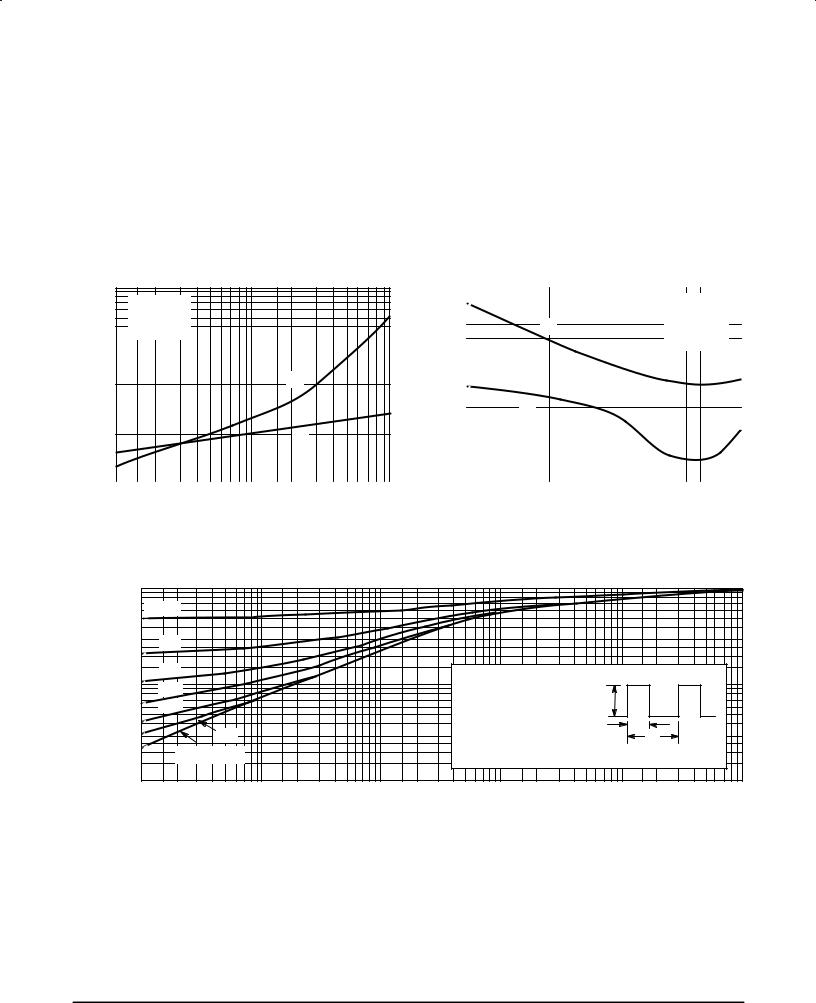
Figure 8. Turn±On Time |
Figure 9. Turn±Off Time |
|
THERMAL RESISTANCE (NORMALIZED) |
1.0 |
|
|
|
|
|
|
|
|
|
|
|
|
|
|
|
|
|
|
|
|
|
0.7 |
D = 0.5 |
|
|
|
|
|
|
|
|
|
|
|
|
|
|
|
|
|
|
||
|
0.5 |
|
|
|
|
|
|
|
|
|
|
|
|
|
|
|
|
|
|
|||
r(t), EFFECTIVE TRANSIENT |
|
|
|
|
|
|
|
|
|
|
|
|
|
|
|
|
|
|
|
|
||
0.3 |
|
0.2 |
|
|
|
|
|
|
|
|
|
|
|
|
|
|
|
|
|
|
||
|
|
|
|
|
|
|
|
|
|
|
|
|
|
|
|
|
|
|
|
|||
0.2 |
|
|
|
|
|
|
|
|
|
|
|
|
|
|
|
|
|
|
|
|
||
0.1 |
|
0.1 |
|
|
|
|
|
|
|
|
RθJC = r(t) θJC |
|
|
|
P(pk) |
|
|
|
|
|||
|
0.05 |
|
|
|
|
|
|
|
|
|
|
|
|
|
|
|
||||||
0.07 |
|
|
|
|
|
|
|
|
|
RθJC = 1.17°C/W MAX |
|
|
|
|
|
|
||||||
|
0.02 |
|
|
|
|
|
|
|
|
|
|
|
|
|
|
|||||||
|
|
|
|
|
|
|
|
|
D CURVES APPLY FOR POWER |
|
|
|
|
|
||||||||
0.05 |
|
|
|
|
|
|
|
|
|
|
|
|
|
|
||||||||
|
|
|
|
|
|
|
|
|
|
|
|
|
|
|
||||||||
|
|
|
|
|
|
|
|
|
|
PULSE TRAIN SHOWN |
|
|
t1 |
|
|
|
||||||
0.03 |
|
|
0.01 |
|
|
|
|
|
|
|
|
|
|
|
|
|||||||
|
|
|
|
|
|
|
|
|
READ TIME AT t1 |
|
|
|
t2 |
|
|
|
||||||
0.02 |
|
SINGLE PULSE |
|
|
|
|
|
|
|
TJ(pk) ± TC = P(pk) RθJC(t) |
|
DUTY CYCLE, D = t1/t2 |
|
|||||||||
|
|
|
|
|
|
|
|
|
|
|
|
|
|
|
|
|
||||||
|
|
0.01 |
|
0.02 0.03 |
0.05 |
0.1 |
0.2 |
0.3 |
0.5 |
1.0 |
2.0 |
3.0 |
5.0 |
10 |
20 |
30 |
50 |
100 |
200 |
300 |
500 |
1000 |
|
|
0.01 |
||||||||||||||||||||
|
|
|
|
|
|
|
|
|
|
|
t, TIME (ms) |
|
|
|
|
|
|
|
|
|
||
Figure 10. Thermal Response
Motorola Bipolar Power Transistor Device Data |
5 |
Смотрите также:
| Концептуальные полки |