Материал: MJE16106
MJE16106
DYNAMIC SATURATION VOLTAGE
For bipolar power transistors low DC saturation voltages are achieved by conductivity modulating the collector region. Since conductivity modulation takes a finite amount of time, DC saturation voltages are not achieved instantly at turn±on. In bridge circuits, two transistor forward converters, and two transistor flyback converters dynamic saturation characteristics are responsible for the bulk of dynamic losses. The MJE16106 has been designed specifically to minimize these losses. Performance is roughly four times better than the original version of MJ16006.
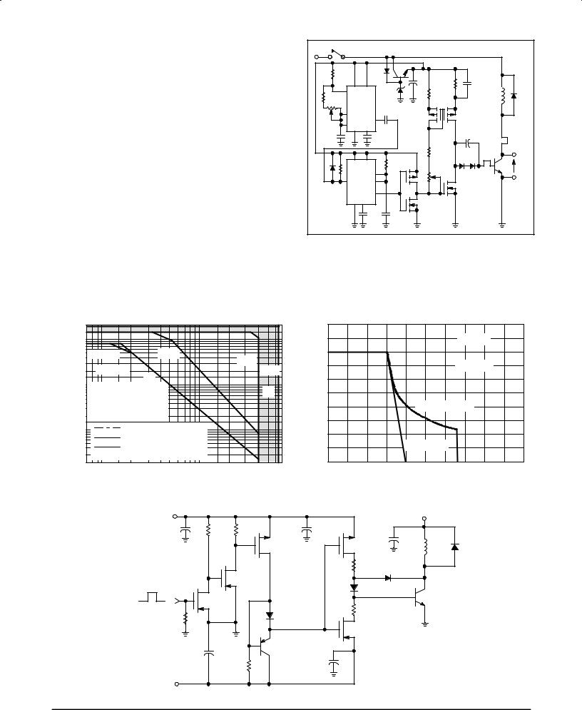
From a measurement point of view, dynamic saturation voltage is defined as collector±emitter voltage at a specific point in time after IB1 has been applied, where t = 0 is the 90% point on the IB1 rise time waveform. This definition is illustrated in Figure 11. Performance data was taken in the circuit that is shown in Figure 13. The 24 volt rail allows a Tektronix 2445 or equivalent scope to operate at 1 volt per division without input amplifier saturation.
Dynamic saturation performance is illustrated in Figure 12. The MJE16106 reaches DC saturation levels in approximately 2 μs, provided that sufficient base drive is provided. The dependence of dynamic saturation voltage upon base drive suggests a spike of IB1 at turn±on to minimize dynamic saturation losses, and also avoid overdrive at turn±off. However, in order to simulate worst case conditions the guaranteed dynamic saturation limits in this data sheet are specified with a constant level of IB1.
+ 24 |
|
|
|
|
|
|
|
|
|
|
|
|
|
|
Q1 |
MJ11012 |
|
|
|
|
|
1 k |
|
|
1N5314 |
|
|
|
|
|
|
|
|
|
|
|
|
|
|
|
|
|
|
|
|
4 |
8 |
|
100 |
2.4 |
Ω |
0.01 |
μF |
|
|
|
|
μF |
20 W |
|
|||||
|
|
|
|
1N4111 |
|
|
|
|||
1 k |
7 |
|
|
|
100 Ω |
|
|
2.4 mH |
1N5831 |
|
|
|
|
|
1 W |
|
|
||||
|
|
|
|
|
|
|
||||
10 k |
|
U1 |
|
|
|
|
|
|
|
|
|
6 |
MC1455 |
100 pF |
Q4 |
|
|
Q5 |
|
|
|
|
(OSCILLATOR) |
|
|
|
|
|||||
|
2 |
3 |
IRFD9120 |
|
|
MTM8P08 |
|
|
||
|
|
|
|
|
|
|
|
|
|
|
0.1 μF |
|
1 |
5 |
|
|
|
|
10 μF |
|
|
|
|
0.01 μF |
|
|
|
|
I C |
|||
|
|
|
|
|
|
|
|
|
|
|
|
|
|
|
|
|
47 Ω |
|
|
|
|
|
|
4 |
8 |
1.8 k |
1 W |
|
MUR405 |
I B |
|
|
|
|
|
|
|
|
T.U.T. |
|
|||
1N914 |
|
|
|
|
IRFD9123 |
500 Ω |
|
|
VCE |
|
|
|
|
7 |
|
|
MUR405 |
|
|||
10 |
k |
U2 |
|
Q2 |
|
|
|
|
|
|
|
2 |
MC1455 |
6 |
|
|
|
Q6 |
|
|
|
|
(25 |
μs) |
|
|
|
|
|
|||
|
|
|
|
|
|
MTP25N06 |
|
|
||
|
|
|
|
|
|
|
|
|
|
|
|
|
|
|
3 |
Q3 |
|
|
|
|
|
|
|
|
|
|
|
|
|
|
|
|
|
|
1 |
5 |
|
IRFD113 |
|
|
|
|
|
|
|
|
|
0.01 μF |
|
|
|
|
|
|
|
|
|
0.01 μF |
|
|
|
|
|
|
|
Figure 13. Dynamic Saturation Test Circuit
|
|
|
|
|
GUARANTEED SAFE OPERATING AREA INFORMATION |
|
|
|
|
|
||||||||||||
|
20 |
|
|
|
|
|
|
|
|
|
|
20 |
|
|
|
|
|
|
|
|
|
|
(AMPS) |
10 |
|
|
|
|
|
|
|
|
|
(AMPS) |
18 |
|
|
|
|
|
|
IC/IB1 = 5 |
|
|
|
7 |
|
|
|
|
|
|
|
|
|
|
|
|
|
|
|
|
|
|
|
|
||
|
5 |
MJE16106 |
|
1.0 ms |
|
|
|
10 μs |
|
|
16 |
|
|
|
|
|
|
|
|
|
|
|
CURRENT |
3 |
REGION II Ð EXPANDED |
|
|
|
II |
CURRENT |
10 |
|
|
|
|
|
|
TJ ≤ 100°C |
|
|
|||||
0.7 |
|
|
|
|
|
|
|
|
|
|
|
|
||||||||||
|
2 |
TC |
= 25°C |
dc |
|
|
|
|
|
100 ns |
|
14 |
|
|
|
|
|
|
|
|
||
|
1 |
|
|
|
|
|
|
|
|
|
12 |
|
|
|
|
|
|
|
|
|
|
|
COLLECTOR |
|
|
|
|
|
|
|
|
|
COLLECTOR |
|
|
|
|
|
|
|
|
|
|
|
|
0.1 |
|
WIRE BOND LIMIT |
|
|
|
|
|
4 |
|
|
|
|
|
|
|
|
|
|
||||
|
0.5 |
FBSOA USING MUR870 |
|
|
|
|
|
|
8 |
|
|
|
|
VBE(off) = 1 to 5 V |
|
|
|
|||||
|
0.3 |
ULTRAFAST RECTIFIER |
|
|
|
|
|
|
6 |
|
|
|
|
|
|
|
||||||
|
0.2 |
(SEE FIGURE 16) |
|
|
|
|
|
|
|
|
|
|
|
|
|
|
|
|
|
|
||
, |
|
|
THERMAL LIMIT |
|
|
|
|
|
, |
|
|
|
|
|
|
|
|
|
|
|
||
C 0.07 |
|
|
|
|
|
|
C |
2 |
|
|
|
|
|
|
|
|
|
|
||||
I |
0.05 |
|
SECONDARY BREAKDOWN |
|
|
|
I |
|
|
|
VBE(off) = 0 V |
|
|
|
|
|||||||
|
|
|
|
|
|
|
|
|
|
|
|
|
|
|||||||||
|
0.03 |
|
LIMIT |
|
|
|
|
|
|
|
|
0 |
|
|
|
|
|
|
|
|
|
|
|
0.02 |
10 |
20 |
30 |
50 |
70 |
|
200 |
300 |
500 650 |
|
|
|
|
|
|
600 |
700 |
800 |
900 |
1K |
|
|
7 |
100 |
|
0 |
100 |
200 |
300 |
400 |
500 |
|||||||||||||
|
|
|
VCE, COLLECTOR±EMITTER VOLTAGE (VOLTS) |
|
|
|
|
VCE, COLLECTOR±EMITTER VOLTAGE (VOLTS) |
|
|
||||||||||||
Figure 14. Maximum Rated Forward Bias |
|
Figure 15. Maximum Rated Reverse Bias |
|||||
Safe Operating Area |
|
|
|
Safe Operating Area |
|||
+15 |
|
|
|
|
|
VCE (650 V MAX) |
|
1.0 μF |
150 Ω 100 Ω |
100 μF |
|
|
|
||
|
|
|
|
|
|||
|
|
MTP8P10 |
|
|
10 μF |
|
|
|
|
|
MTP8P10 |
10 mH |
MUR870 |
||
|
|
|
|
RB1 |
MUR170 |
|
|
|
MPF930 |
|
|
|
|
|
|
|
|
|
|
|
|
|
|
+10 |
|
|
|
MUR105 |
|
|
|
MPF930 |
|
|
|
|
T.U.T. |
|
|
|
|
|
|
|
|
||
50 Ω |
|
MUR105 |
|
RB2 |
|
|
|
|
|
|
|
|
|
||
|
|
|
|
|
|
|
|
|
|
|
|
MTP12N10 |
|
|
|
|
500 μF |
MJE210 |
|
|
|
|
|
|
|
|
|
|
|
|
|
|
150 Ω |
1 |
μF |
|
Note: Test Circuit for Ultra±fast FBSOA |
||
|
|
|
|
||||
|
|
|
|
|
Note: RB2 = 0 and VOff = ± 5 Volts |
||
VOff |
|
|
|
|
|
|
|
|
Figure 16. Switching Safe Operating Area |
|
|
||||
6 |
|
|
|
Motorola Bipolar Power Transistor Device Data |
|||
POWER DERATING FACTOR (%)
100
80
60
40
20
0
0
MJE16106
SECOND BREAKDOWN
DERATING
THERMAL
DERATING
40 |
80 |
120 |
160 |
200 |
|
TC, CASE TEMPERATURE (°C) |
|
|
|
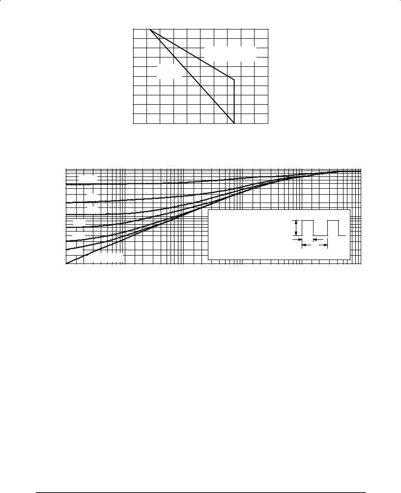
Figure 17. Power Derating
|
|
1 |
|
|
|
|
|
|
|
|
|
|
|
|
|
|
|
TRANSIENT THERMAL RESISTANCE |
|
0.7 |
D = 0.5 |
|
|
|
|
|
|
|
|
|
|
|
|
|
|
|
0.5 |
|
|
|
|
|
|
|
|
|
|
|
|
|
|||
|
|
|
|
|
|
|
|
|
|
|
|
|
|
|
|
||
|
0.3 |
|
0.2 |
|
|
|
|
|
|
|
|
|
|
|
|
|
|
(NORMALIZED) |
0.2 |
|
|
|
|
|
|
|
|
|
|
|
|
|
|
||
|
|
|
|
|
|
|
|
|
|
|
|
|
|
|
|||
0.1 |
|
0.1 |
|
|
|
|
|
|
|
|
|
P(pk) |
|
|
|
||
|
|
|
|
|
|
|
ZθJC(t) = r(t) RθJC |
|
|
|
|
|
|||||
0.07 |
0.05 |
|
|
|
|
|
|
° |
|
|
|
|
|
||||
0.05 |
|
|
|
|
|
|
|
RθJC = 1.0 OR 1.25 C/W MAX |
|
|
|
|
|
||||
0.02 |
|
|
|
|
|
|
D CURVES APPLY FOR POWER |
|
|
|
|
|
|||||
0.03 |
|
|
|
|
|
|
PULSE TRAIN SHOWN |
|
t1 |
|
|
|
|||||
|
|
|
|
|
|
|
|
|
|
|
|||||||
|
|
|
|
|
|
|
READ TIME AT t1 |
|
|
t2 |
|
|
|||||
0.02 |
|
|
|
|
|
|
|
|
|
|
|
|
|||||
r(t), |
|
0.01 |
|
|
|
|
|
|
TJ(pk) ± TC = P(pk) ZθJC |
|
DUTY CYCLE, D = t1/t2 |
|
|||||
|
|
SINGLE PULSE |
|
|
|
|
|
|
|||||||||
|
|
|
|
|
|
|
|
|
|
|
|
|
|||||
|
|
0.01 |
|
|
|
|
|
|
|
|
|
|
|
|
|
||
|
|
0.02 |
0.05 |
0.1 |
0.2 |
0.5 |
1 |
2 |
5 |
10 |
20 |
50 |
100 |
200 |
500 |
1.0 k |
|
|
|
0.01 |
|||||||||||||||
t, TIME (ms)
Figure 18. Typical Thermal Response [ZθJC(t)]
SAFE OPERATING AREA INFORMATION
FORWARD BIAS
There are two limitations on the power handling ability of a transistor: average junction temperature and second breakdown. Safe operating area curves indicate IC ± VCE limits of the transistor that must be observed for reliable operation; i.e., the transistor must not be subjected to greater dissipation than the curves indicate.
The data in Figure 14 is based on TC = 25_C; TJ(pk) is variable depending on power level. Second breakdown pulse
limits are valid for duty cycles to 10% but must be derated when TC ≥ 25_C. Second breakdown limitations do not derate the same as thermal limitations. Allowable current at the voltages shown on Figure 14 may be found at any case temperature by using the appropriate curve on Figure 17.
TJ(pk) may be calculated from the data in Figure 18. At high case temperatures, thermal limitations will reduce the power
that can be handled to values less than the limitations imposed by second breakdown.
REVERSE BIAS
For inductive loads, high voltage and high current must be sustained simultaneously during turn±off, in most cases, with
the base±to±emitter junction reverse biased. Under these conditions the collector voltage must be held to a safe level at or below a specific value of collector current. This can be accomplished by several means such as active clamping, RC snubbing, load line shaping, etc. The safe level for these devices is specified as Reverse Biased Safe Operating Area and represents the voltage±current condition allowable during reverse biased turn±off. This rating is verified under clamped conditions so that the device is never subjected to an avalanche mode. Figure 15 gives the RBSOA characteristics.
SWITCHMODE III DESIGN CONSIDERATIONS
FBSOA
Allowable dc power dissipation in bipolar power transistors decreases dramatically with increasing collector±emitter voltage. A transistor which safely dissipates 100 watts at 10 volts will typically dissipate less than 10 watts at its rated
V(BR)CEO(sus). From a power handling point of view, current and voltage are not interchangeable (see Application Note
AN875).
Motorola Bipolar Power Transistor Device Data |
7 |

MJE16106
TURN±ON
Safe turn±on load line excursions are bounded by pulsed FBSOA curves. The 10 μs curve applies for resistive loads, most capacitive loads, and inductive loads that are clamped by standard or fast recovery rectifiers. Similarly, the 100 ns curve applies to inductive loads which are clamped by ultra± fast recovery rectifiers, and are valid for turn±on crossover times less than 100 ns (AN952).
At voltages above 75% of V(BR)CEO(sus), it is essential to provide the transistor with an adequate amount of base
drive VERY RAPIDLY at turn±on. More specifically, safe operation according to the curves is dependent upon base current rise time being less than collector current rise time. As a general rule, a base drive compliance voltage in excess of 10 volts is required to meet this condition (see Application Note AN875).
TURN±OFF
A bipolar transistor's ability to withstand turn±off stress is dependent upon its forward base drive. Gross overdrive violates the RBSOA curve and risks transistor failure. For this reason, circuits which use fixed base drive are more likely to fail at light loads due to heavy overdrive (see Application Note AN875).
OPERATION ABOVE V(BR)CEO(sus)
When bipolars are operated above collector±emitter breakdown, base drive is crucial. A rapid application of ade-
quate forward base current is needed for safe turn±on, as is a stiff negative bias needed for safe turn±off. Any hiccup in the base±drive circuitry that even momentarily violates either of these conditions will likely cause the transistor to fail. Therefore, it is important to design the driver so that its output is negative in the absence of anything but a clean crisp input signal (see Application Note AN952).
RBSOA
Reversed Biased Safe Operating Area has a first order dependency on circuit configuration and drive parameters. The RBSOA curves in this data sheet are valid only for the conditions specified. For a comparison of RBSOA results in several types of circuits (see Application Note AN951).
DESIGN SAMPLES
Transistor parameters tend to vary much more from wafer lot to wafer lot, over long periods of time, than from one device to the next in the same wafer lot. For design evaluation it is advisable to use transistors from several different date codes.
BAKER CLAMPS
Many unanticipated pitfalls can be avoided by using Baker Clamps. MUR105 and MUR170 diodes are recommended for base drives less than 1 amp. Similarly, MUR405 and MUR470 types are well±suited for higher drive requirements (see Article Reprint AR131).
8 |
Motorola Bipolar Power Transistor Device Data |
MJE16106
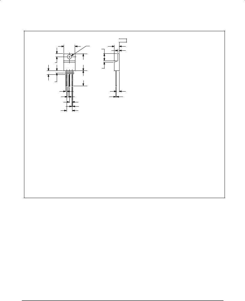
PACKAGE DIMENSIONS
|
|
|
|
±T± |
|
B |
|
F |
C |
|
|
|
T |
S |
4 |
|
|
|
|
Q |
|
|
A |
|
1 |
2 |
3 |
U |
|
H |
|
|
|
|
Z |
|
|
K |
|
|
|
|
|
|
L |
|
|
|
R |
V |
|
|
|
J |
G |
|
|
|
|
|
|
|
D |
|
|
N |
|
|
|
SEATING PLANE
NOTES:
1.DIMENSIONING AND TOLERANCING PER ANSI Y14.5M, 1982.
2.CONTROLLING DIMENSION: INCH.
3.DIMENSION Z DEFINES A ZONE WHERE ALL BODY AND LEAD IRREGULARITIES ARE ALLOWED.
|
INCHES |
MILLIMETERS |
||
DIM |
MIN |
MAX |
MIN |
MAX |
A |
0.570 |
0.620 |
14.48 |
15.75 |
B |
0.380 |
0.405 |
9.66 |
10.28 |
C |
0.160 |
0.190 |
4.07 |
4.82 |
D |
0.025 |
0.035 |
0.64 |
0.88 |
F |
0.142 |
0.147 |
3.61 |
3.73 |
G |
0.095 |
0.105 |
2.42 |
2.66 |
H |
0.110 |
0.155 |
2.80 |
3.93 |
J |
0.018 |
0.025 |
0.46 |
0.64 |
K |
0.500 |
0.562 |
12.70 |
14.27 |
L |
0.045 |
0.060 |
1.15 |
1.52 |
N |
0.190 |
0.210 |
4.83 |
5.33 |
Q |
0.100 |
0.120 |
2.54 |
3.04 |
R |
0.080 |
0.110 |
2.04 |
2.79 |
S |
0.045 |
0.055 |
1.15 |
1.39 |
T |
0.235 |
0.255 |
5.97 |
6.47 |
U |
0.000 |
0.050 |
0.00 |
1.27 |
V |
0.045 |
±±± |
1.15 |
±±± |
Z |
±±± |
0.080 |
±±± |
2.04 |
STYLE 1:
PIN 1. BASE
2.COLLECTOR
3.EMITTER
4.COLLECTOR
CASE 221A±06
TO±220AB
ISSUE Y
Motorola Bipolar Power Transistor Device Data |
9 |

MJE16106
Motorola reserves the right to make changes without further notice to any products herein. Motorola makes no warranty, representation or guarantee regarding the suitability of its products for any particular purpose, nor does Motorola assume any liability arising out of the application or use of any product or circuit, and specifically disclaims any and all liability, including without limitation consequential or incidental damages. ªTypicalº parameters can and do vary in different applications. All operating parameters, including ªTypicalsº must be validated for each customer application by customer's technical experts. Motorola does not convey any license under its patent rights nor the rights of others. Motorola products are not designed, intended, or authorized for use as components in systems intended for surgical implant into the body, or other applications intended to support or sustain life, or for any other application in which the failure of the Motorola product could create a situation where personal injury or death may occur. Should Buyer purchase or use Motorola products for any such unintended or unauthorized application, Buyer shall indemnify and hold Motorola and its officers, employees, subsidiaries, affiliates, and distributors harmless against all claims, costs, damages, and expenses, and reasonable attorney fees arising out of, directly or indirectly, any claim of personal injury or death associated with such unintended or unauthorized use, even if such claim alleges that Motorola was negligent regarding the design or manufacture of the part. Motorola and  are registered trademarks of Motorola, Inc. Motorola, Inc. is an Equal Opportunity/Affirmative Action Employer.
How to reach us: |
|
USA / EUROPE: Motorola Literature Distribution; |
JAPAN: Nippon Motorola Ltd.; Tatsumi±SPD±JLDC, Toshikatsu Otsuki, |
P.O. Box 20912; Phoenix, Arizona 85036. 1±800±441±2447 |
6F Seibu±Butsuryu±Center, 3±14±2 Tatsumi Koto±Ku, Tokyo 135, Japan. 03±3521±8315 |
MFAX: RMFAX0@email.sps.mot.com ± TOUCHTONE (602) 244±6609 HONG KONG: Motorola Semiconductors H.K. Ltd.; 8B Tai Ping Industrial Park, |
|
INTERNET: http://Design±NET.com |
51 Ting Kok Road, Tai Po, N.T., Hong Kong. 852±26629298 |
◊ MJE16106/D
*MJE16106/D*