Материал: mocz500rev2
MOTOROLA
SEMICONDUCTOR TECHNICAL DATA
Order this document by MOCZ500/D
GlobalOptoisolator |
Mini Zero-Crossing AC SSR
MOCZ500
Motorola Preferred Device
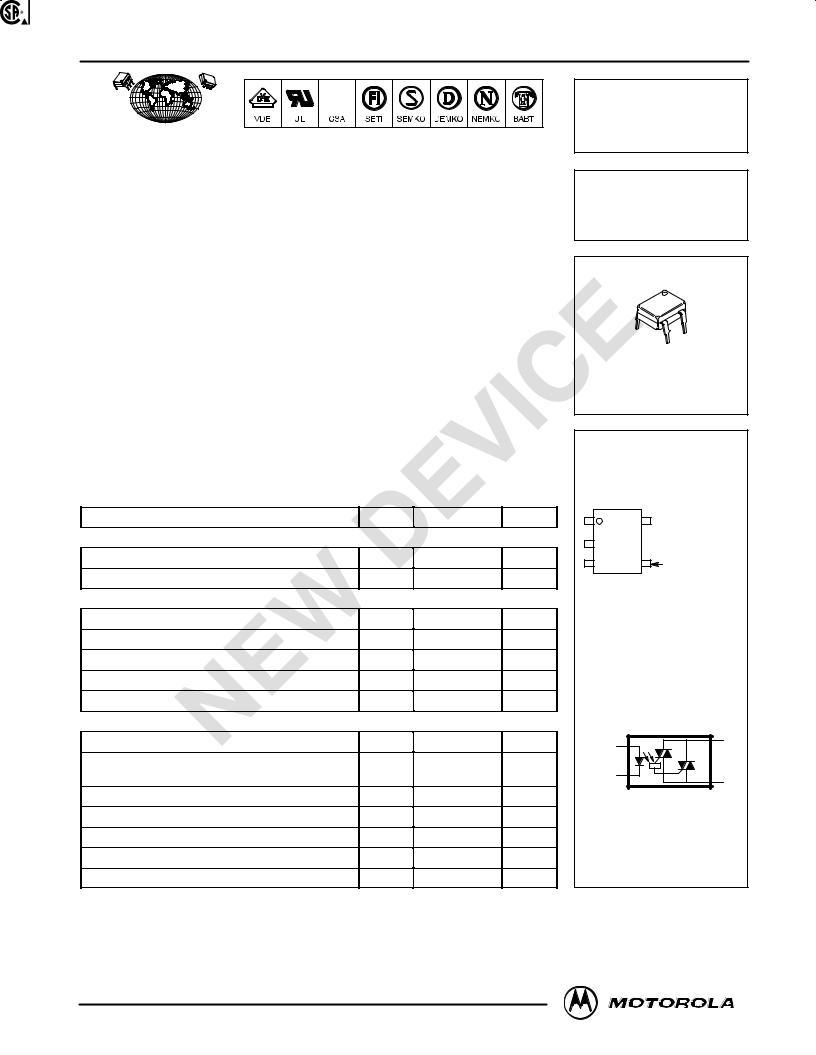
This device consists of a gallium arsenide infrared emitting diode optically |
OPTOISOLATOR |
|
coupled to a zero±cross triac circuit and a power triac. It is capable of driving |
||
ZERO CROSS |
||
loads up to 500 mA rms on AC voltages from 20 to 280 V rms. |
||
TRIAC OUTPUT |
||
|
•Provides Normally Open AC Output with 500 mA Rating @ 40_C
•Small Outline, Standard 6±PIN DIP Package
•Simplified Logic Control of 240 Vac Power
•High Input±Output Isolation of 7500 Vac (rms)
• 7 Amp Single Cycle Surge Capability |
|
|
|
|
|
|
|
• Wide Load Power Factor Range 0.1±1 |
|
|
|
|
|
|
|
• Low Input/Output Capacitance |
|
|
|
|
|
|
|
Applications: |
|
|
|
|
CASE 730J±01 |
||
• Logic to AC Line Interface |
• Appliance Solenoids |
|
|
||||
|
|
STYLE 1 |
|||||
• Microprocessor to AC Line Peripheral |
• Appliance Actuators |
|
|
||||
|
|
|
|
||||
• Industrial Controls |
• Appliance Fan Motors |
|
|
|
|
||
• EM Relays and Contactors |
• Appliance Lights |
|
|
|
|
||
• Small AC Motor Drives |
|
|
|
|
|
|
|
• Incandescent Lamp Drive |
|
|
|
|
PINOUT |
||
|
|
|
|
|
|||
MAXIMUM RATINGS (TA = 25°C unless otherwise noted) |
|
|
1 |
6 |
1. LED Anode |
||
Rating |
Symbol |
Value |
Unit |
||||
2. LED Cathode |
|||||||
|
|
||||||
INPUT LED |
|
|
|
2 |
|
3. Not Connected |
|
|
|
|
|
4. MT2 |
|||
|
|
|
|
MOCZ500 |
6. MT1 |
||
Reverse Voltage |
VR |
6 |
V |
3 |
4 |
||
Connected to |
|||||||
Forward Current Ð Continuous |
IF |
50 |
mA |
|
|
Internal Triac |
|
|
|
|
|
|
|
Heat Spreader |
|
OUTPUT TRIAC |
|
|
|
|
|
|
|
Off±State Output Terminal Voltage (1) |
VDRM |
600 |
V |
|
|
|
|
Peak Repetitive Surge Current (1 Cycle) |
ITSM |
7 |
A |
|
|
|
|
Main Terminal Fusing Current (t = 8.3 ms) |
I2T |
0.4 |
A2sec |
|
|
|
|
On±State Current Range |
IT(rms) |
0.030 to 0.500 |
A |
|
COUPLER |
||
|
SCHEMATIC |
||||||
Load Power Factor Range |
pF |
0.1 ± 1.0 |
Ð |
|
|||
|
|
|
|||||
TOTAL DEVICE |
|
|
|
|
LED Drive Triac |
||
Isolation Surge Voltage (2) |
VISO |
7500 |
Vac(pk) |
1 |
|
6 |
|
|
MT1 |
||||||
Total Power Dissipation @ TA = 40°C |
|
|
|
Anode |
|
|
|
PD |
600 |
mW |
Cathode 2 |
|
|
||
(Device Soldered on PCB) |
|
|
|
* |
4 |
||
|
|
|
°C |
|
|
MT2 |
|
Junction Temperature Range |
TJ |
± 40 to +125 |
* ZERO VOLTAGE |
|
|||
Ambient Operating Temperature Range |
TA |
± 40 to +85 |
°C |
|
|||
* ACTIVATION |
|
||||||
Ambient Operating Relative Humidity @ TA = 85°C |
RHA |
85 |
% |
|
|
|
|
Storage Temperature Range |
Tstg |
± 40 to +125 |
°C |
|
|
|
|
Soldering Temperature (10 sec) |
TL |
260 |
°C |
|
|
|
|
1. Test voltages must be applied within dv/dt rating. |
|
|
|
|
|
|
|
2. Input±Output isolation voltage, VISO. is an internal device dielectric breakdown rating. For this test, |
|
|
|
||||
pins 1 and 2 are common and pins 4 and 6 are common. |
|
|
|
|
|
||
Preferred devices are Motorola recommended choices for future use and best overall value. |
|
|
|
|
|||
REV 2 |
|
|
|
|
|
|
|
Motorola Optoelectronics Device Data |
|
|
|
|
|
1 |
|
Motorola, Inc. 1997 |
|
|
|
|
|
|
|

MOCZ500
THERMAL CHARACTERISTICS
Characteristic |
Symbol |
|
Value |
|
Unit |
|
|
|
|
|
|
Thermal Resistance, Junction to Air |
RθJA |
|
130 |
|
_C/W |
(Device Soldered on PCB) |
|
|
|
|
|
|
|
|
|
|
|
Thermal Resistance, Junction to Case (Pin 4) |
RθJC |
|
40 |
|
_C/W |
(Device Soldered on PCB) |
|
|
|
|
|
|
|
|
|
|
|
ELECTRICAL CHARACTERISTICS (TA = 25°C unless otherwise noted) |
|
|
|
|
|
|
|
|
|
|
|
Characteristic |
Symbol |
Min |
Typ |
Max |
Unit |
|
|
|
|
|
|
INPUT LED |
|
|
|
|
|
|
|
|
|
|
|
Reverse Leakage Current (VR = 6 V) |
IR |
Ð |
0.05 |
100 |
μA |
Forward Voltage (IF = 10 mA) |
VF |
Ð |
1.2 |
1.5 |
V |
OUTPUT TRIAC |
|
|
|
|
|
|
|
|
|
|
|
Leakage with LED Off @ TA = 85°C |
IDRM |
Ð |
Ð |
100 |
μA |
(VDRM = 600 V) |
|
|
|
|
|
Critical Rate of Rise of Off±State Voltage (Static) (1) |
dv/dt(s) |
Ð |
2,000 |
Ð |
V/μs |
(Vp = 400 V) |
|
|
|
|
|
|
|
|
|
|
|
LED On, Driver Holding Current |
IH1 |
Ð |
150 |
500 |
μA |
COUPLED |
|
|
|
|
|
|
|
|
|
|
|
LED Trigger Current Required to Latch Output (2) (3) |
IFT(on) |
Ð |
Ð |
10 |
mA |
(Main Terminal Voltage = 5 V) |
|
|
|
|
|
|
|
|
|
|
|
On±State Voltage (IT = 500 mA) |
VTM |
Ð |
1.2 |
1.5 |
V |
Inhibit Voltage (IF = IFT) |
VINH |
Ð |
10 |
20 |
V |
Commutating dv/dt |
dv/dt (c) |
10 |
Ð |
Ð |
V/μs |
|
|
|
|
|
|
Common±Mode Input±Output dv/dt |
dv/dt (cm) |
40,000 |
Ð |
Ð |
V/μs |
|
|
|
|
|
|
Input±Output Capacitance |
CISO |
Ð |
Ð |
1 |
pF |
Isolation Resistance @ 500 Vdc |
RISO |
1012 |
Ð |
Ð |
Ohms |
1.Additional dv/dt information, including test methods, can be found in Motorola applications note AN1048/D, Figure 40.
2.All devices are guaranteed to trigger at as IF value less than or equal to the max IFT. Therefore, the recommended operating IF lies between the device's maximum IFT(on) limit and the Maximum Rating of 60 mA.
3.Current±limiting resistor required in series with LED.
ENVIRONMENTAL TEST REQUIREMENTS
Test |
Test Conditions |
|
|
Autoclave |
TA = 121°C, RH = 100%, P = 15 PSIG, 48 Hr. |
Moisture Resistance |
Mil±Std±883, Method 1004 |
|
|
Temp Cycle |
TA = ±40/+125°C, Air to Air, Dwell w15 min., Transfer v5 min., 200 Cycles |
Resistance to Solder Heat |
Mil±Std±750, Method 2031, 260°C followed by VISO |
Lead Pull |
Mil±Std±750, Method 2036, Condition A, 2 lbs., 1 min. |
|
|
LIFE TEST REQUIREMENTS
|
Test Conditions |
|
|
|
|
|
|
Test |
Environment |
Bias |
Duration |
|
|
|
|
High Temperature, Reverse Bias |
TA = +100°C |
VTM = 280 Vac |
1000 Hr. |
High Humidity, High Temperature, Reverse Bias |
TA = +85°C |
VTM = 100 Vdc |
500 Hr. |
|
RH = 85% |
Pin 4 = + |
|
|
|
Pin 6 = ± |
|
|
|
|
|
Intermittent Operating Life |
ton = 2 min. |
IF = 50 mA |
1000 Hr. |
|
toff = 2 min. |
ITM = 60 mA |
|
|
TA = +25°C |
|
|
ESD |
Human Body Model & Machine Models 1 & 2 |
N/A |
N/A |
|
|
|
|
2 |
Motorola Optoelectronics Device Data |
MOCZ500
TYPICAL ELECTRICAL CHARACTERISTICS
|
60 |
|
|
|
|
|
|
|
(mA) |
50 |
|
|
|
|
|
|
|
|
|
|
|
|
|
|
|
|
CURRENT |
40 |
|
|
|
|
|
|
|
|
|
|
|
|
|
|
|
|
LED |
30 |
|
|
|
|
|
|
|
|
|
|
|
|
|
|
|
|
, FORWARD |
20 |
|
|
|
|
|
|
|
10 |
|
|
|
|
|
|
|
|
F |
|
|
|
|
|
|
|
|
I |
|
|
|
|
|
|
|
|
|
0 |
± 20 |
0 |
20 |
40 |
60 |
80 |
100 |
|
± 40 |
|||||||
|
|
|
TA, AMBIENT TEMPERATURE (°C) |
|
|
|||
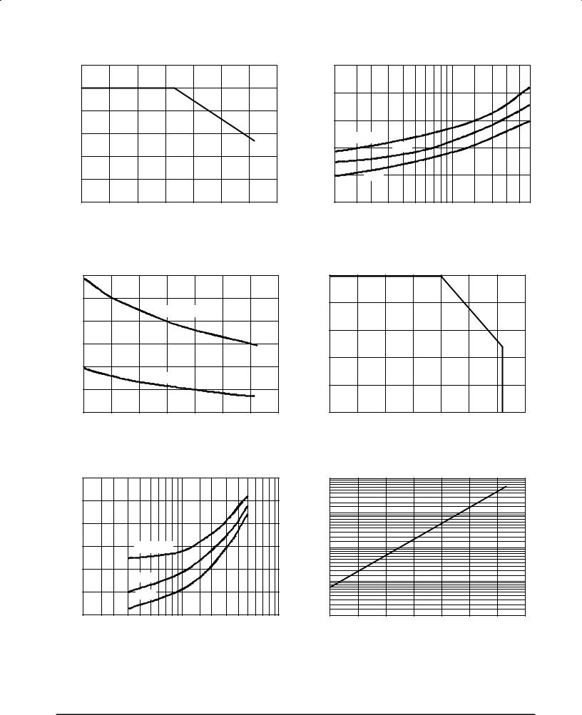
Figure 1. Maximum Allowable Forward LED
Current versus Ambient Temperature
IT = IT Max
|
1.8 |
|
(V) |
1.6 |
|
|
|
|
VOLTAGE |
1.4 |
|
|
|
|
, FORWARD |
1.2 |
TA = ± 40°C |
° |
||
|
25 C |
|
|
|
|
F |
|
|
V |
1 |
85°C |
|
||
|
0.8 |
|
|
1 |
10 |
IF, FORWARD CURRENT (mA)
Figure 2. LED Forward Voltage versus LED Forward Current
(mA) |
14 |
|
|
|
|
|
|
|
|
500 |
|
|
|
|
|
|
|
12 |
|
|
|
|
|
|
|
|
|
|
|
|
|
|
|
|
|
CURRENTTRIGGER |
|
|
|
|
|
|
|
(mA)CURRENTTERMINAL |
400 |
|
|
|
|
|
|
|
|
|
|
|
|
|
|
|
|
|
|
|
|
|
|
|
|||
|
|
|
|
|
|
|
|
|
|
|
|
|
|
|
|
|
|
|
10 |
|
|
GUARANTEED |
|
|
|
|
|
|
|
|
|
|
|
|
|
|
|
|
|
|
|
|
|
|
|
|
|
|
|
|
|
|
|
|
|
|
|
|
|
|
|
|
|
300 |
|
|
|
|
|
|
|
|
8 |
|
|
|
|
|
|
|
|
|
|
|
|
|
|
|
|
FORWARD |
|
|
|
|
|
|
|
|
I |
200 |
|
|
|
|
|
|
|
6 |
|
|
|
|
|
|
|
|
|
|
|
|
|
|
|
||
|
|
|
|
|
|
|
|
|
|
|
|
|
|
|
|
|
|
|
|
|
|
TYPICAL |
|
|
|
|
, |
|
|
|
|
|
|
|
|
|
4 |
|
|
|
|
|
|
|
T |
100 |
|
|
|
|
|
|
|
|
|
|
|
|
|
|
|
|
|
|
|
|
|
|
|
||
, |
|
|
|
|
|
|
|
|
|
|
|
|
|
|
|
|
|
FT |
|
|
|
|
|
|
|
|
|
|
|
|
|
|
|
|
|
I |
|
|
|
|
|
|
|
|
|
|
|
|
|
|
|
|
|
|
2 |
|
|
|
|
|
|
|
|
0 |
|
|
|
|
|
|
|
|
± 40 |
± 20 |
0 |
20 |
40 |
60 |
80 |
100 |
|
± 40 |
± 20 |
0 |
20 |
40 |
60 |
80 |
100 |
|
|
|
TA, AMBIENT TEMPERATURE (°C) |
|
|
|
|
|
TA, AMBIENT TEMPERATURE (°C) |
|
|
||||||
Figure 3. Forward Trigger Current versus |
Figure 4. RMS ON±State Current versus |
Ambient Temperature |
Ambient Temperature |
VTM, MAIN TERMINAL VOLTAGE (V)
1.4 |
|
|
|
10 |
|
|
|
|
|
|
|
1.3 |
|
|
(μA) |
|
|
|
|
|
|
|
|
|
|
|
1 |
|
|
|
|
|
|
|
|
|
|
|
CURRENT |
|
|
|
|
|
|
|
|
1.2 |
|
|
|
|
|
|
|
|
|
|
|
|
|
|
|
|
|
|
|
|
|
|
|
1.1 |
TA = ± 40°C |
|
LEAKAGE |
0.1 |
|
|
|
|
|
|
|
1 |
25°C |
|
0.01 |
|
|
|
|
|
|
|
|
|
|
, |
|
|
|
|
|
|
|
||
0.9 |
85°C |
|
DRM |
|
|
|
|
|
|
|
|
|
I |
|
|
|
|
|
|
|
|
||
|
|
|
|
|
|
|
|
|
|
|
|
0.8 |
|
|
|
0.001 |
|
|
|
|
|
|
|
0.01 |
0.1 |
1 |
|
± 40 |
± 20 |
0 |
20 |
40 |
60 |
80 |
100 |
|
ITM, MAIN TERMINAL CURRENT (A) |
|
|
|
|
TA, AMBIENT TEMPERATURE (°C) |
|
|
|||
|
Figure 5. Main Terminal Voltage versus Main |
|
|
|
Figure 6. Typical Leakage Current versus |
|
|||||
|
Terminal Current |
|
|
|
|
Ambient Temperature |
|
|
|||
Motorola Optoelectronics Device Data |
3 |
MOCZ500
TYPICAL ELECTRICAL CHARACTERISTICS (continued)
|
300 |
|
|
|
|
|
|
|
μA) |
250 |
|
|
|
|
|
|
|
|
|
|
|
|
|
|
|
|
( |
|
|
|
|
|
|
|
|
CURRENT |
200 |
|
|
|
|
|
|
|
|
|
|
|
|
|
|
|
|
, HOLDING |
150 |
|
|
|
|
|
|
|
|
|
|
|
|
|
|
|
|
H |
100 |
|
|
|
|
|
|
|
I |
|
|
|
|
|
|
|
|
|
50 |
|
|
|
|
|
|
|
|
± 40 |
± 20 |
0 |
20 |
40 |
60 |
80 |
100 |
|
|
|
TA, AMBIENT TEMPERATURE (°C) |
|
|
|||
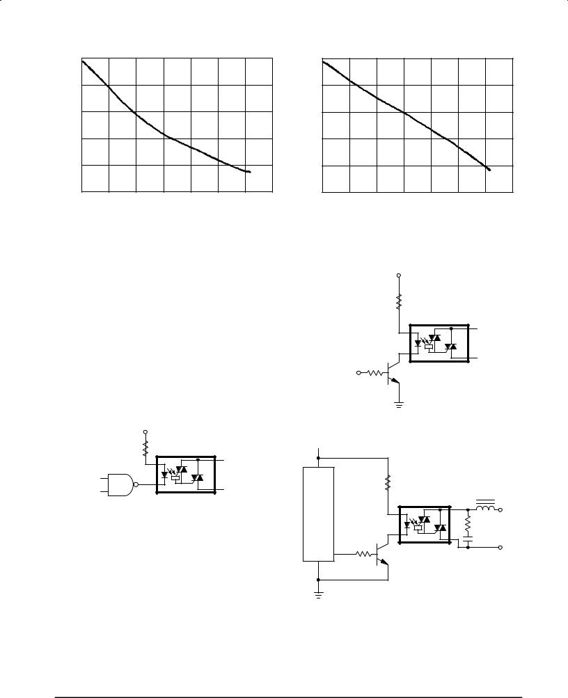
Figure 7. Holding Current versus
Ambient Temperature
|
11.5 |
|
|
|
|
|
|
|
(V) |
11 |
|
|
|
|
|
|
|
|
|
|
|
|
|
|
|
|
VOLTAGE |
10.5 |
|
|
|
|
|
|
|
|
|
|
|
|
|
|
|
|
, INHIBIT |
10 |
|
|
|
|
|
|
|
|
|
|
|
|
|
|
|
|
IH |
|
|
|
|
|
|
|
|
V |
9.5 |
|
|
|
|
|
|
|
|
|
|
|
|
|
|
|
|
|
9 |
|
|
|
|
|
|
|
|
± 40 |
± 20 |
0 |
20 |
40 |
60 |
80 |
100 |
|
|
|
TA, AMBIENT TEMPERATURE (°C) |
|
|
|||
Figure 8. Inhibit Voltage versus
Ambient Temperature
APPLICATION CONSIDERATIONS
Input Drive Circuit
The MOCZ500 SSR is guaranteed to trigger with an input current of 10 mA at 25°C. This trigger current increases with lower ambient temperatures as shown on Figure 3 Forward Trigger Current (IFT) versus Ambient Temperature.
When the input drive circuit is capable to supply the MOCZ500 input LED trigger current, only a current limiting resistor in series with the LED is required. TTL, DTL and microcontrollers with enhanced current capability output ports are able to meet this requirement.
Most CMOS logic circuits and Microcontroller output ports are not rated to sink or source currents required to trigger the MOCZ500. In this case a drive circuit is required as shown in Figure 10 or a TTL buffer interface circuit as shown in Figure 9.
VCC
R1 |
TTI/DTL
R1 for VCC (low) 4.5 V, IFT = 10 mA, VF LED = 1.2 V, VOL = 0.5 V R1 = (4.5 V ± 1.2 V ± 0.5 V): 10 mA = 280 Ω
Choose 270 Ω
Figure 9. Input Drive Circuit
Snubber Circuit
Snubberless operation of resistive loads is possible, but snubbers are recommended for all applications. A typical application is shown in Figure 11. The snubber attenuates the high kickback voltages and commutating dv/dt generated by inductive loads during the turn off of the SSR. It also protects the SSR from line transients generated elsewhere within the equipment (for example inductive loads switched by mechanical contacts such as relays manual on/off switches etc.) or outside the equipment such as air conditioners, electrical heaters and motors.
|
VCC |
|
R1 |
|
MOCZ500 |
|
R2 |
Vin |
Q1 |
Figure 10. Noninverting Discrete NPN Buffer
and Level Shifter
 VCC
VCC
R1 |
μP |
R2 |
Q1 |
MOCZ500 |
LOAD |
|
|
|
|
|
Rs |
AC LINE |
|
|
|
|
Cs |
|
Buffer Circuit
R1 = (VCC ± VFLED ± Vsat Q1): IF MOCZ500 R2 = 10 kΩ
Q1 = General Purpose Trans. NPN Typical Snubber circuit:
For inductive and resistive loads Rs = 45 Ω Cs = 0.01 μF
Figure 11. Typical Application with an μP Output Buffer
4 |
Motorola Optoelectronics Device Data |
Snubbers are also necessary to pass noise immunity tests such as IEC1000 4±4 for fast transients. In this test fast rising high voltage spikes are superimposed onto the line voltage to simulate AC line transients.
Switching Loads with Currents Below the Minimum Current Rating
The MOCZ500 is capable to switch any inductive or resistive load within its rating of minimum 30 mA and a maximum of 500 mA RMS.
MOCZ500
At operating currents below the minimum specified value the Power triac remains in the off state and the triac driver carries the current. This may cause a problem, because the triac driver has a significant lower commutating dv/dt than the power triac. For loads below 30 mA AC rms a snubber is mandatory. Evaluations with various low current inductive and resistive loads concluded that a snubber of R = 100 Ω and C = 10 nF is sufficient.
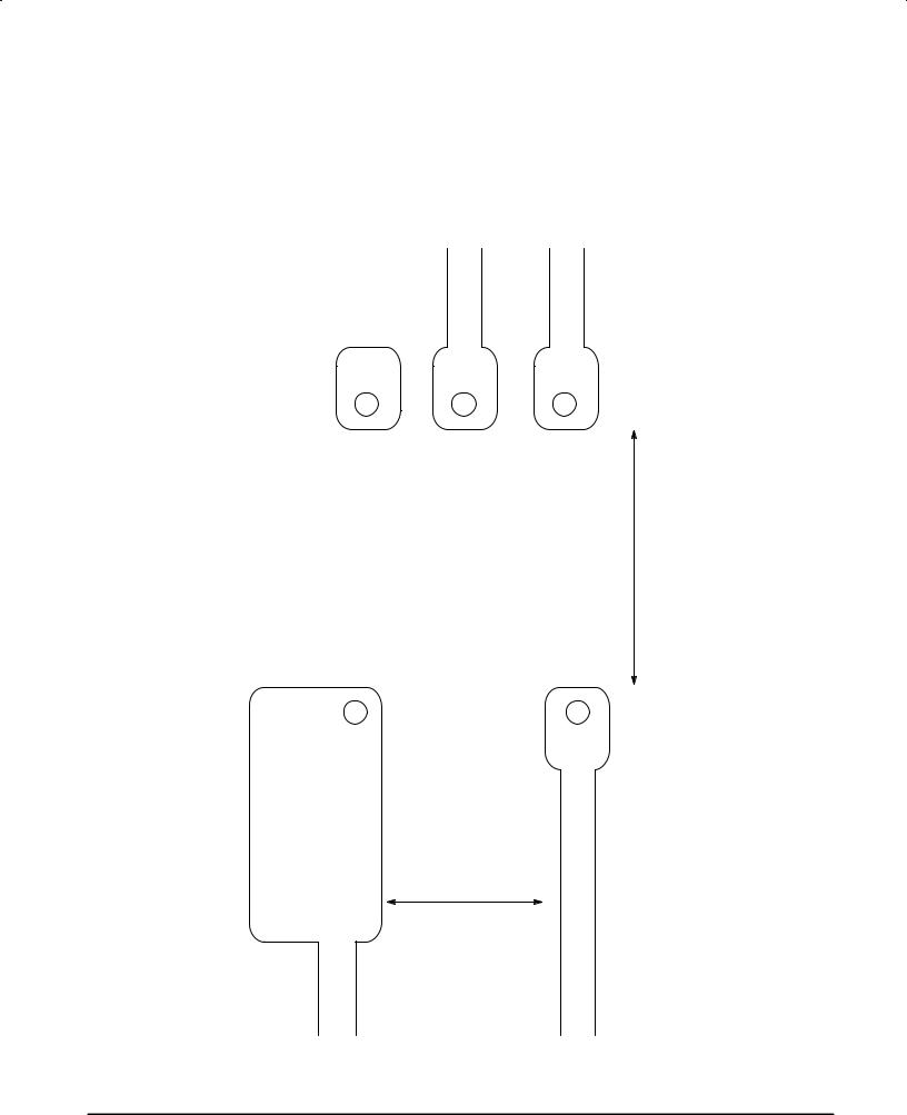
PAD FOR POWER
DISSIPATION
CREEPAGE AND CLEARANCE DISTANCE FOR SAFE ISOLATION (8mm FOR APPLIANCES)
ENLARGED PAD FOR
IMPROVED POWER
DISSIPATION
CREEPAGE AND CLEARANCE
DISTANCE FOR FUNCTIONAL
ISOLATION
(3.5mm APPLIANCES JAPAN)
Figure 12.
Motorola Optoelectronics Device Data |
5 |