Материал: mocz500rev2
MOCZ500
Thermal Considerations
Heat generated inside the MOCZ500's power triac is transferred through the leads to the circuit board where it is dissipated. It is therefore important to solder all leads to the circuit board. Pin 4 is thermally and electrically direct connected to the Power triac and carries the highest amount of thermal energy. For loads which approach the maximum current rating of the SSR it is advisable to layout the pad size for pin 4 as large as possible. See Figure 12 which considers thermal and Regulatory requirements on a PCB.
Regulatory Safety Considerations
The MOCZ500 is designed to meet the National and International Regulatory requirements for safe isolation
between input and output and functional isolation creepage and clearance distances between the AC output pins.
Many equipment standards demand a creepage and clearance distance between input and output circuit of 8mm and a thickness through insulation of 0.4mm (16 mil). All Motorola Optocouplers do meet the thickness through insulation requirement. Product with lead bend option ªTº meets the creepage path requirement. The most stringent requirement for creepage and clearance between the AC output pins is 3.5mm. Figure 12 shows a PCB pattern layout which meets the regulatory requirements for 115 Vrms and 240 Vrms supply line applications.
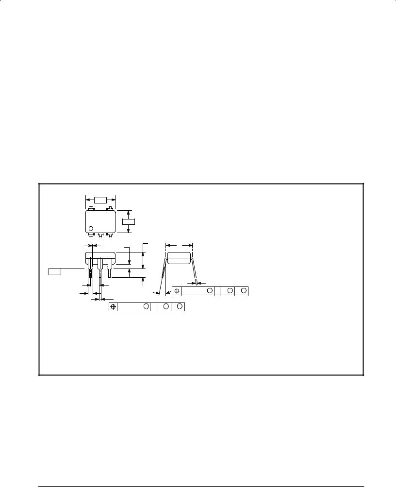
OUTLINE DIMENSIONS
±A±
6 |
4 |
|
|
|
±B± |
|
|
1 |
3 |
|
|
F 4 PL |
C |
L |
|
N |
|||
±T± SEATING |
K |
|
|
PLANE |
|
|
|
G |
|
J 5 PL |
|
M |
0.13 (0.005) M T B M A M |
||
E 5 PL |
|||
D 5 PL |
|
||
|
|
||
|
0.13 (0.005) M T A M |
B M |
NOTES:
1.DIMENSIONING AND TOLERANCING PER ANSI Y14.5M, 1982.
2.CONTROLLING DIMENSION: INCH.
3.DIMENSION L TO CENTER OF LEAD WHEN FORMED PARALLEL.
|
INCHES |
MILLIMETERS |
||
DIM |
MIN |
MAX |
MIN |
MAX |
A |
0.320 |
0.350 |
8.13 |
8.89 |
B |
0.240 |
0.260 |
6.10 |
6.60 |
C |
0.115 |
0.200 |
2.93 |
5.08 |
D |
0.016 |
0.020 |
0.41 |
0.50 |
E |
0.040 |
0.070 |
1.02 |
1.77 |
F |
0.010 |
0.014 |
0.25 |
0.36 |
G |
0.100 BSC |
2.54 BSC |
||
J |
0.008 |
0.012 |
0.21 |
0.30 |
K |
0.100 |
0.150 |
2.54 |
3.81 |
L |
0.300 BSC |
7.62 BSC |
||
M |
0 |
15 |
0 |
15 |
N |
0.015 |
0.100 |
0.38 |
2.54 |
STYLE 1:
PIN 1. LED ANODE
2.LED CATHODE
3.NC
4.MAIN TERMINAL
5.ABSENT
6.MAIN TERMINAL
CASE 730J±01
ISSUE O
6 |
Motorola Optoelectronics Device Data |
MOCZ500
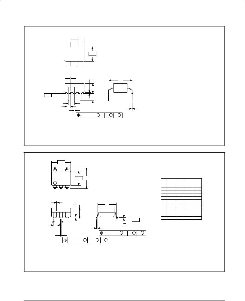
OUTLINE DIMENSIONS (continued)

 ±A±
±A± 
6 4
±B±
 1 3
1 3
|
F 4 PL |
N |
C |
|
|
|
|
L |
|
|
|
|
|
|
|||
±T± |
SEATING |
|
K |
|
|
|
|
|
|
PLANE |
|
|
|
|
|
|
|
|
E 5 PL |
G |
|
|
|
|
|
|
|
D 5 PL |
|
|
|
|
|
J |
|
|
|
|
|
|
|
|
||
|
|
|
|
|
|
|
|
|
|
|
0.13 (0.005) M |
T |
A |
M |
B |
M |
|
NOTES:
1.DIMENSIONING AND TOLERANCING PER ANSI Y14.5M, 1982.
2.CONTROLLING DIMENSION: INCH.
3.DIMENSION L TO CENTER OF LEAD WHEN FORMED PARALLEL.
|
INCHES |
MILLIMETERS |
||
DIM |
MIN |
MAX |
MIN |
MAX |
A |
8.13 |
8.89 |
0.320 |
0.350 |
B |
6.10 |
6.60 |
0.240 |
0.260 |
C |
2.93 |
5.08 |
0.115 |
0.200 |
D |
0.41 |
0.50 |
0.016 |
0.020 |
E |
1.02 |
1.77 |
0.040 |
0.070 |
F |
0.25 |
0.36 |
0.010 |
0.014 |
G |
2.54 BSC |
0.100 BSC |
||
J |
0.21 |
0.30 |
0.008 |
0.012 |
K |
2.54 |
3.81 |
0.100 |
0.150 |
L |
10.16 |
10.80 |
0.400 |
0.425 |
N |
0.38 |
1.02 |
0.015 |
0.040 |
STYLE 1:
PIN 1. LED ANODE
2.LED CATHODE
3.NC
4.MAIN TERMINAL
5.ABSENT
6.MAIN TERMINAL
CASE 730K±01
ISSUE O
|
±A± |
|
|
NOTES: |
|
|
1. |
DIMENSIONING AND TOLERANCING PER ANSI |
6 |
4 |
Y14.5M, 1982. |
|
2. |
CONTROLLING DIMENSION: INCH. |
|
±B± |
S |
|
|
|
|
|
|
|
|
|
|
|
INCHES |
MILLIMETERS |
||
1 |
3 |
|
|
|
|
|
|
|
|
|
|
|
|
||||
|
|
|
|
|
|
|
|
|
|
DIM |
MIN |
MAX |
MIN |
MAX |
|||
|
|
|
|
|
|
|
|
|
|
|
|
||||||
|
|
|
|
|
|
|
|
|
|
|
|
A |
0.320 |
0.350 |
8.13 |
8.89 |
|
|
|
|
|
|
|
|
|
|
|
|
|
B |
0.240 |
0.260 |
6.10 |
6.60 |
|
|
|
|
|
|
|
|
|
|
|
|
|
C |
0.115 |
0.200 |
2.93 |
5.08 |
|
|
|
|
|
|
|
|
|
|
|
|
|
D |
0.016 |
0.020 |
0.41 |
0.50 |
|
|
|
|
|
|
|
|
|
|
|
|
|
E |
0.040 |
0.070 |
1.02 |
1.77 |
|
F 4 PL |
|
|
|
|
|
|
L |
|
|
|
|
F |
0.010 |
0.014 |
0.25 |
0.36 |
|
H |
C |
|
|
|
|
|
|
|
|
G |
|
0.100 BSC |
2.54 BSC |
||||
|
|
|
|
|
|
|
|
|
H |
0.020 |
0.025 |
0.51 |
0.63 |
||||
|
|
|
|
|
|
|
|
|
|
|
|
||||||
|
|
|
|
|
|
|
|
|
|
|
|
J |
0.008 |
0.012 |
0.20 |
0.30 |
|
|
|
|
|
|
|
|
|
|
|
|
|
K |
0.006 |
0.035 |
0.16 |
0.88 |
|
|
|
|
|
|
|
|
|
|
|
|
|
L |
|
0.320 BSC |
8.13 BSC |
||
|
|
|
|
|
|
|
|
|
|
±T± |
S |
0.332 |
0.390 |
8.43 |
9.90 |
||
|
G |
|
|
|
|
|
|
|
|
|
|
|
|
|
|
||
E 5 PL |
|
|
|
|
|
|
|
J |
SEATING |
|
|
|
|
|
|
||
|
|
|
|
|
|
|
|
|
|
|
|
|
|
||||
|
|
|
|
|
|
K 5 PL |
|
|
PLANE |
|
STYLE 1: |
|
|
|
|
||
|
|
|
|
|
|
|
|
|
|
|
LED ANODE |
|
|
||||
|
|
|
|
|
|
|
0.13 (0.005) M |
T |
B |
|
A |
PIN 1. |
|
|
|||
|
D 5 PL |
|
|
|
|
|
M |
M |
2. |
LED CATHODE |
|
|
|||||
|
|
|
|
|
|
|
|
|
|
|
|
3. |
NC |
|
|
|
|
|
0.13 (0.005) M |
T |
A |
M |
B |
M |
|
|
|
|
|
4. |
MAIN TERMINAL |
|
|||
|
|
|
|
|
|
5. |
ABSENT |
|
|
||||||||
|
|
|
|
|
|
|
|
|
|
|
|
|
6. |
MAIN TERMINAL |
|
||
CASE 730L±01
ISSUE A
Motorola Optoelectronics Device Data |
7 |

MOCZ500
Motorola reserves the right to make changes without further notice to any products herein. Motorola makes no warranty, representation or guarantee regarding the suitability of its products for any particular purpose, nor does Motorola assume any liability arising out of the application or use of any product or circuit, and specifically disclaims any and all liability, including without limitation consequential or incidental damages. ªTypicalº parameters which may be provided in Motorola data sheets and/or specifications can and do vary in different applications and actual performance may vary over time. All operating parameters, including ªTypicalsº must be validated for each customer application by customer's technical experts. Motorola does not convey any license under its patent rights nor the rights of others. Motorola products are not designed, intended, or authorized for use as components in systems intended for surgical implant into the body, or other applications intended to support or sustain life, or for any other application in which the failure of the Motorola product could create a situation where personal injury or death may occur. Should Buyer purchase or use Motorola products for any such unintended or unauthorized application, Buyer shall indemnify and hold Motorola and its officers, employees, subsidiaries, affiliates, and distributors harmless against all claims, costs, damages, and expenses, and reasonable attorney fees arising out of, directly or indirectly, any claim of personal injury or death associated with such unintended or unauthorized use, even if such claim alleges that Motorola was negligent regarding the design or manufacture of the part. Motorola and  are registered trademarks of Motorola, Inc. Motorola, Inc. is an Equal Opportunity/Affirmative Action Employer.
|
Mfax is a trademark of Motorola, Inc. |
How to reach us: |
|
USA / EUROPE / Locations Not Listed: Motorola Literature Distribution; |
JAPAN: Nippon Motorola Ltd.; Tatsumi±SPD±JLDC, 6F Seibu±Butsuryu±Center, |
P.O. Box 5405, Denver, Colorado 80217. 303±675±2140 or 1±800±441±2447 |
3±14±2 Tatsumi Koto±Ku, Tokyo 135, Japan. 81±3±3521±8315 |
Mfax : RMFAX0@email.sps.mot.com ± TOUCHTONE 602±244±6609 |
ASIA/PACIFIC: Motorola Semiconductors H.K. Ltd.; 8B Tai Ping Industrial Park, |
± US & Canada ONLY 1±800±774±1848 51 Ting Kok Road, Tai Po, N.T., Hong Kong. 852±26629298
INTERNET: http://www.mot.com/SPS/
8 |
◊ |
MOCZ500/D |
|
Motorola Optoelectronics Device Data |