Материал: mrf5015rev6d
DESIGN CONSIDERATIONS
The MRF5015 is a common±source, RF power, N±Channel enhancement mode, Metal±Oxide Semiconductor Field± Effect Transistor (MOSFET). Motorola RF MOSFETs feature a vertical structure with a planar design. Motorola Application Note AN211A, ªFETs in Theory and Practice,º is suggested reading for those not familiar with the construction and characteristics of FETs.
This device was designed primarily for 12.5 volt VHF and UHF power amplifier applications. The major advantages of RF power MOSFETs include high gain, simple bias systems, relative immunity from thermal runaway, and the ability to withstand severely mismatched loads without suffering damage.
MOSFET CAPACITANCES
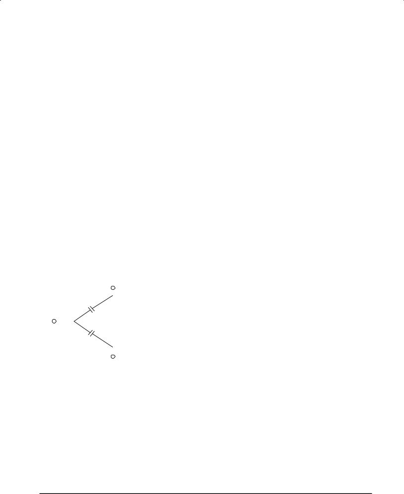
The physical structure of a MOSFET results in capacitors between all three terminals. The metal oxide gate structure determines the capacitors from gate±to±drain (Cgd), and gate±to±source (Cgs). The PN junction formed during fabrication of the RF MOSFET results in a junction capacitance from drain±to±source (Cds). These capacitances are characterized as input (Ciss), output (Coss) and reverse transfer (Crss) capacitances on data sheets. The relationships between the inter±terminal capacitances and those given on data sheets are shown below. The Ciss can be specified in two ways:
1.Drain shorted to source and positive voltage at the gate.
2.Positive voltage of the drain in respect to source and zero volts at the gate.
In the latter case, the numbers are lower. However, neither method represents the actual operating conditions in RF applications.
|
|
|
|
|
Drain |
|
|
|
Cgd |
|
|
||
Gate |
|
Ciss = Cgd + Cgs |
||||
|
|
|
|
|
Cds |
Coss = Cgd + Cds |
|
|
|
|
|
||
|
|
|
|
|
|
Crss = Cgd |
|
|
Cgs |
|
|
||
|
|
|
|
|
Source |
|
|
|
|
|
|
|
|
|
|
|
|
|
|
|
DRAIN CHARACTERISTICS
One critical figure of merit for a FET is its static resistance in the full±on condition. This on±resistance, Rds(on), occurs in the linear region of the output characteristic and is specified at a specific gate±source voltage and drain current. The drain±source voltage under these conditions is termed
Vds(on). For MOSFETs, Vds(on) has a positive temperature coefficient at high temperatures because it contributes to the
power dissipation within the device.
GATE CHARACTERISTICS
The gate of the RF MOSFET is a polysilicon material, and is electrically isolated from the source by a layer of oxide. The input resistance is very high, on the order of 109 Ω, resulting in a leakage current of a few nanoamperes.
Gate control is achieved by applying a positive voltage to the gate greater than the gate±to±source threshold voltage,
VGS(th).
Gate Voltage Rating ± Never exceed the gate voltage rating. Exceeding the rated VGS can result in permanent damage to the oxide layer in the gate region.
Gate Termination ± The gates of these devices are essentially capacitors. Circuits that leave the gate open±circuited or floating must be avoided. These conditions can result in turn±on of the devices due to voltage build±up on the input capacitor due to leakage currents or pickup.
Gate Protection ± These devices do not have an internal monolithic zener diode from gate±to±source. If gate protection is required, an external zener diode is recommended with appropriate RF decoupling networks.
Using a resistor to keep the gate±to±source impedance low also helps dampen transients and serves another important function. Voltage transients on the drain can be coupled to the gate through the parasitic gate±drain capacitance. If the gate±to±source impedance and the rate of voltage change on the drain are both high, then the signal coupled to the gate may be large enough to exceed the gate±threshold voltage and turn the device on.
DC BIAS
Since the MRF5015 is an enhancement mode FET, drain current flows only when the gate is at a higher potential than the source. See Figure 5 for a typical plot of drain current versus gate voltage. RF power FETs operate optimally with a quiescent drain current (IDQ), whose value is application dependent. The MRF5015 was characterized at IDQ = 100 mA, which is the suggested value of bias current for typical applications. For special applications such as linear amplification, IDQ may have to be selected to optimize the critical parameters.
The gate is a dc open circuit and draws essentially no current. Therefore, the gate bias circuit may generally be just a simple resistive divider network. Some special applications may require a more elaborate bias system.
GAIN CONTROL
Power output of the MRF5015 may be controlled to some degree with a low power dc control signal applied to the gate, thus facilitating applications such as manual gain control, ALC/AGC and modulation systems. Figure 4 is an example of output power variation with gate±source bias voltage with Pin held constant. This characteristic is very dependent on frequency and load line.
MRF5015 |
MOTOROLA RF DEVICE DATA |
6 |
|

AMPLIFIER DESIGN
Impedance matching networks similar to those used with bipolar transistors are suitable for the MRF5015. For examples see Motorola Application Note AN721, ªImpedance Matching Networks Applied to RF Power Transistors.º Both small±signal S±parameters and large±signal impedances are provided. While the S±parameters will not produce an exact design solution for high power operation, they do yield a good first approximation. This is an additional advantage of RF power MOSFETs.
Since RF power MOSFETs are triode devices, they are not unilateral. This coupled with the very high gain of MRF5015
yield a device quite capable of self oscillation. Stability may be achieved by techniques such as drain loading, input shunt resistive loading, or output to input feedback. Different stabilizing techniques may be required depending on the desired gain and bandwidth of the application. The RF test fixture implements a parallel resistor and capacitor in series with the gate to improve stability and input impedance Q.
Two port stability analysis with the MRF5015 S±parameters provides a useful tool for selection of loading or feedback circuitry to assure stable operation. See Motorola Application Note AN215A, ªRF Small±Signal Design Using Two±Port Parameters,º for a discussion of two port network theory and stability.
MOTOROLA RF DEVICE DATA |
MRF5015 |
|
7 |
|
|
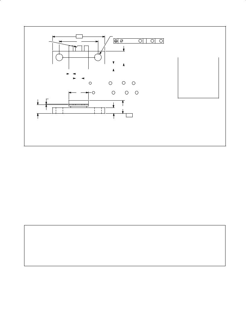
PACKAGE DIMENSIONS |
|
|
|
|
-A- |
Q 2 PL |
|
|
|
IDENTIFICATION |
L |
0.15 (0.006) M |
T A M |
N M |
|
NOTCH |
|
|
|
NOTES: |
|
|
|
|
|
||
6 |
5 |
4 |
|
1. |
DIMENSIONING AND TOLERANCING PER |
|
|
ANSI Y14.5M, 1982. |
|||
|
|
|
|
|
|
|
|
|
|
2. |
CONTROLLING DIMENSION: INCH. |
|
|
|
|
|
|
|
|
|
|
|
|
|
|
|
|
|
|
|
|
|
|
|
|
|
|
|
|
|
|
-N- |
|
|
|
|
|
|
|
|
|
|
||
|
|
|
|
|
|
|
|
|
|
|
|
|
|
|
|
|
|
|
|
|
|
|
|
|
|
|
|
|
|
|
|
|
|
|
|
|
|
|
INCHES |
MILLIMETER |
||
|
|
|
|
|
|
|
|
|
|
|
|
|
|
|
|
|
|
|
|
|
|
|
|
|
|
|
|
|
|
|
|
|
|
|
|
|
|
DIM |
MIN |
MAX |
MIN |
MAX |
|
1 |
|
2 |
|
3 |
|
|
|
|
|
|
|
|
|
|
|
|
K |
|
|
|
|
|
|
|
|
|
|
A |
0.965 |
0.985 |
24.52 |
25.01 |
|||||||||
|
|
|
|
|
|
|
|
|
|
|
|
|
|
|
|
|
|
|
|
|
|
|
|
|
|
|
|
|
|
|
|
|
|
|
B |
0.355 |
0.375 |
9.02 |
9.52 |
|||
|
|
|
|
|
|
|
|
|
|
|
|
|
|
|
|
|
|
|
|
|
|
|
|
|
|
|
|
|
|
|
|
|
|
|
|
|
|
C |
0.230 |
0.260 |
5.85 |
6.60 |
|
|
F |
|
|
|
|
|
|
|
|
|
|
|
|
|
|
|
|
|
|
|
|
|
|
|
|
|
|
|
|
|
|
|
|
|
D |
0.115 |
0.125 |
2.93 |
3.17 |
||
|
|
|
|
|
|
|
|
|
|
|
|
|
|
|
|
|
|
|
|
|
|
|
|
|
|
|
|
|
|
|
|
|
|
|||||||||
|
|
|
|
|
|
|
|
|
|
|
|
|
|
D 2 PL |
|
|
|
|
|
|
|
|
|
|
E |
0.102 |
0.114 |
2.59 |
2.90 |
|||||||||||||
|
|
|
|
|
|
|
|
|
|
|
|
|
|
|
|
|
|
|
|
|
|
|
|
F |
0.075 |
0.085 |
1.91 |
2.15 |
||||||||||||||
|
|
|
|
|
|
|
|
|
|
|
|
|
|
|
|
|
|
|
|
|
|
|
|
|||||||||||||||||||
|
|
|
|
|
|
|
|
|
|
|
|
|
|
|
|
|
|
|
0.38 (0.015) M |
T |
A |
M |
|
N M |
|
|
H |
0.160 |
0.170 |
4.07 |
4.31 |
|||||||||||
|
|
|
|
|
|
|
|
|
|
|
|
|
|
|
|
|
|
|
|
|
||||||||||||||||||||||
|
|
|
|
|
|
|
|
|
|
|
|
|
|
|
|
|
J |
0.004 |
0.006 |
0.11 |
0.15 |
|||||||||||||||||||||
|
|
|
|
|
|
|
|
|
|
|
|
|
|
|
|
|
|
|
|
|
|
|
|
|
|
|
|
|
|
|
|
|
|
|
|
|
|
|||||
|
|
|
|
|
|
|
|
|
|
|
|
|
|
|
|
|
|
|
|
|
|
|
|
|
|
|
|
|
|
|
|
|
|
|
|
|
|
K |
0.090 |
0.110 |
2.29 |
2.79 |
|
|
|
|
|
|
|
|
|
B |
|
|
|
|
|
|
|
|
|
|
|
|
|
|
|
|
|
|
|
|
|
|
|
|
|
|
|
L |
0.725 BSC |
18.42 BSC |
|||
|
|
|
|
|
|
|
|
|
|
|
|
|
|
|
|
|
|
|
0.38 (0.015) M |
T |
|
A M |
|
N M |
|
|||||||||||||||||
|
|
|
|
|
|
|
|
|
|
|
|
|
|
|
|
|
|
|
|
|
|
N |
0.225 |
0.241 |
5.72 |
6.12 |
||||||||||||||||
|
|
|
|
|
|
|
|
|
|
|
|
|
|
|
|
|
|
|
|
|
|
|
|
|
|
|
|
|
|
|
|
|
|
|
|
|
|
Q |
0.125 |
0.135 |
3.18 |
3.42 |
|
J |
|
|
|
|
|
|
STYLE 3: |
|
|
C |
|
PIN 1. |
SOURCE (COMMON) |
H |
|
2. |
GATE (INPUT) |
|
E |
|
|||
|
|
3. |
SOURCE (COMMON) |
|
|
-T- |
SEATING |
4. |
SOURCE (COMMON) |
|
5. |
DRAIN (OUTPUT) |
||
|
|
PLANE |
||
|
|
|
6. |
SOURCE (COMMON) |
CASE 319±07
ISSUE M
Motorola reserves the right to make changes without further notice to any products herein. Motorola makes no warranty, representation or guarantee regarding the suitability of its products for any particular purpose, nor does Motorola assume any liability arising out of the application or use of any product or circuit, and specifically disclaims any and all liability, including without limitation consequential or incidental damages. ªTypicalº parameters can and do vary in different applications. All operating parameters, including ªTypicalsº must be validated for each customer application by customer's technical experts. Motorola does not convey any license under its patent rights nor the rights of others. Motorola products are not designed, intended, or authorized for use as components in systems intended for surgical implant into the body, or other applications intended to support or sustain life, or for any other application in which the failure of the Motorola product could create a situation where personal injury or death may occur. Should Buyer purchase or use Motorola products for any such unintended or unauthorized application, Buyer shall indemnify and hold Motorola and its officers, employees, subsidiaries, affiliates, and distributors harmless against all claims, costs, damages, and expenses, and reasonable attorney fees arising out of, directly or indirectly, any claim of personal injury or death associated with such unintended or unauthorized use, even if such claim alleges that Motorola was negligent regarding the design or manufacture of the part. Motorola and  are registered trademarks of Motorola, Inc. Motorola, Inc. is an Equal Opportunity/Affirmative Action Employer.
How to reach us: |
|
USA / EUROPE: Motorola Literature Distribution; |
JAPAN: Nippon Motorola Ltd.; Tatsumi±SPD±JLDC, Toshikatsu Otsuki, |
P.O. Box 20912; Phoenix, Arizona 85036. 1±800±441±2447 |
6F Seibu±Butsuryu±Center, 3±14±2 Tatsumi Koto±Ku, Tokyo 135, Japan. 03±3521±8315 |
MFAX: RMFAX0@email.sps.mot.com ± TOUCHTONE (602) 244±6609 HONG KONG: Motorola Semiconductors H.K. Ltd.; 8B Tai Ping Industrial Park, |
|
INTERNET: http://Design±NET.com |
51 Ting Kok Road, Tai Po, N.T., Hong Kong. 852±26629298 |
◊ |
MRF5015/D |
|
MOTOROLA RF DEVICE DATA |
|
*MRF5015/D* |