Материал: 3

AC TEST CIRCUITS. The following test circuits and conditions represent Motorola's typical test procedures. AC waveforms and terminology can be found on pages 3-8 to 3-10.
Proper testing requires that care be taken in the construction of AC test fixtures. This is especially true of FAST TTL. Maintaining a 50 Ω environment on the ac test fixture, as well as the use of multilayer boards with internal VCC and ground planes is highly recommended for FAST TTL. Bypassing with both electrolytic and high quality RF type capacitors should be provided on the board. Lead lengths for all components should be kept as short as possible (Motorola uses and recommends chip capacitors and resistors for ac test fixtures). Following these rules will result in cleaner waveforms as well as better correlation between Motorola and the FAST TTL consumer.
FUNCTIONAL TESTING OF TTL IN A NOISY ENVIRONMENT/ªDYNAMICº THRESHOLD
Testing noise (noise generated by the test system itself and noise generated by TTL devices under test interacting with the test system) adds to, or subtracts from the threshold voltage applied to the TTL device under test. For this reason Motorola does not recommend functional testing of TTL devices using threshold levels of 0.8 V and 2.0 V. Instead, good TTL testing techniques call for hard levels of less than 0.5 V VIL and greater than 2.4 V VIH to be applied for functional testing. Input threshold voltages should be tested separately, and only (for noise reasons above) after setting the device state with a hard level.
VOH
VOUT |
|
|
|
Trigger |
|
|
|
|||
|
|
|
|
|
||||||
|
|
VOL |
Threshold |
|
|
|||||
|
|
|
||||||||
|
|
|
|
|
|
|
|
|
||
|
|
|
|
|
|
|
|
|
||
|
|
|
|
|
|
|
|
|
|
|
|
|
|
|
|
|
|
|
|
|
|
|
VIN |
|
|
|
|
|
|
Dynamic |
||
|
|
|
|
|
|
|
||||
|
|
|
|
|
|
|
|
|
Threshold |
|
|
|
|
|
Region of output instability; |
|
|||||
|
|
|
|
|
|
|||||
|
|
|
|
|
|
|||||
|
|
|
|
Dynamic Noise contribution to apparent input threshold |
||||||
The VIN versus VOUT plot shows the practical effect of testing noise on a logic IC device. The actual device Trigger threshold is represented by the initial low to high output transition. The device will oscillate if the input voltage does not exceed the trigger threshold plus the noise generated by the interaction of the test system or given application with the device.
The Dynamic threshold (that creates Quiescent outputs), is the input logic level required to overcome the interactive DYNAMIC NOISE generated by a device switching states. The amount of interactive DYNAMIC NOISE can be characterized by the difference between the Trigger threshold and the Dynamic threshold of the device under test. A simple number cannot be assigned to this parameter as it is heavily dependent on any given application or test environment.
So although the Trigger threshold of any given device will correlate well between any test system, the correlation of ªDynamicº threshold cannot be made directly and will have meaning only in a relative sense.
FAST AND LS TTL DATA
3-11
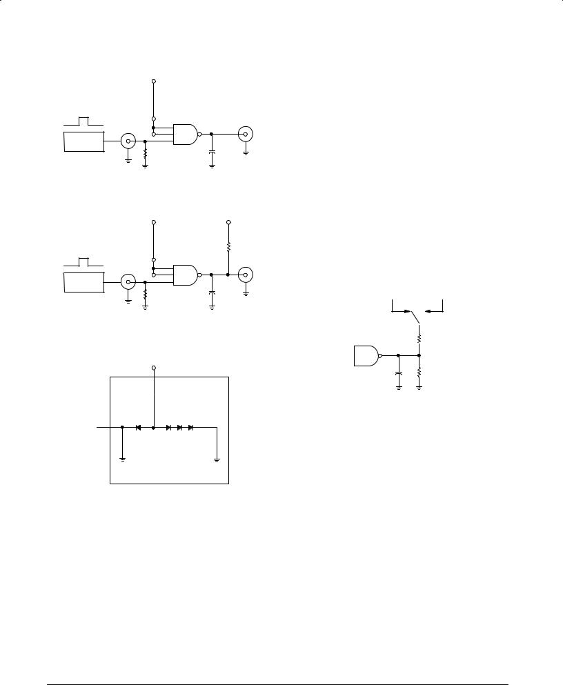
LS TEST CIRCUITS
Test Circuit for Standard Output Devices
VCC
VIN |
DUT |
VOUT |
|
PULSE GEN |
|||
|
|
||
|
51 Ω |
15 pF* |
Test Circuit for Open Collector Output Devices
|
VCC |
VCC |
|
|
|
RL |
|
VIN |
DUT |
VOUT |
|
PULSE GEN |
|||
|
|
||
|
51 Ω |
15 pF* |
*includes all probe and jig capacitance
Optional LS Load (GuaranteedÐNot Tested)
VCC
 RL
RL
 CL
CL
PULSE GENERATOR SETTINGS (UNLESS OTHERWISE SPECIFIED)
|
LS |
FAST |
Frequency = 1 MHz |
1 MHz |
|
Duty Cycle = 50% |
50% |
|
1 TLH (tr) = |
6 ns (15)* |
2.5 ns |
1 THL (tf) = |
6 ns (15)* |
2.5 ns |
Amplitude = |
0 to 3 V |
0 to 3 V |
*The specified propagation delay limits can be guaranteed with a 15 ns input rise time on all parameters except those requiring narrow pulse widths. Any frequency measurement over 15 MHz or pulse width less than 30 ns must be performed with a 6 ns input rise time.
FAST TEST CIRCUITS
+7 V |
OPEN |
tPZL, tPLZ, O.C.  ALL OTHER R1
 500 Ω
500 Ω
DUT
50 pF* |
R2 |
||
500 |
Ω |
||
|
|||
*includes all probe and jig capacitance
FAST AND LS TTL DATA
3-12
APPLICATIONS ASSISTANCE FORM
In the event that you have any questions or concerns about the performance of any Motorola device listed in this catalog, please contact your local Motorola sales office or the Motorola Help line for assistance. If further information is required, you can request direct factory assistance.
Please fill out as much of the form as is possible if you are contacting Motorola for assistance or are sending devices back to Motorola for analysis. Your information can greatly improve the accuracy of analysis and can dramatically improve the correlation response and resolution time.
Items 4 thru 8 of the following form contains important questions that can be invaluable in analyzing application or device problems. It can be used as a self-help diagnostic guideline or for a baseline of information gathering to begin a dialog with Motorola representatives.
MOTOROLA Device Correlation/Component Analysis Request Form
Ð Please fill out entire form and return with devices to MOTOROLA INC., R&QA DEPT., 2200 W. Broadway, Mesa, AZ 85202.
1) |
Name of Person Requesting Correlation: |
|
|
|
|
|
|
|||
|
Phone No: |
|
Job Title: |
|
|
|
Company: |
|
||
2) |
Alternate Contact: |
|
|
|
|
Phone/Position: |
|
|||
3)Device Type (user part number):
4)Industry Generic Device Type:
5)# of devices tested/sampled:
#of devices in question*:
#returned for correlation:
* In the event of 100% failure, does Customer have other date codes of Motorola devices that pass inspection?
Yes |
|
|
No |
|
Please specify passing date code(s) if applicable |
|
|
If none, does customer have viable alternate vendor(s) for device type? |
|||||||
Yes |
|
|
No |
|
Alternate vendor's name |
|
|
6)Date code(s) and Serial Number(s) of devices returned for correlation Ð If possible, please provide one or two ªgoodº units (Motorola's and/or other vendor) for comparison:
7)Describe USER process that device(s) are questionable in:
Incoming component inspection {test system = ?}:
Design prototyping:
Board test/burn-in:
Other (please describe):
8) Please describe the device correlation operating parameters as completely as possible for device(s) in question:
>Describe all pin conditions (e.g. floating, high, low, under test, stimulated but not under test, whatever ...), including any input or output loading conditions (resistors, caps, clamps, driving devices or devices being driven ...). Potentially critical information includes:
Input waveform timing relationships Input edge rates
Input Overshoot or Undershoot Ð Magnitude and Duration Output Overshoot or Undershoot Ð Magnitude and Duration
>Photographs, plots or sketches of relevent inputs and outputs with voltages and time divisions clearly identified for all waveforms are greatly desirable.
>VCC and Ground waveforms should be carefully described as these characteristics vary greatly between applications and test systems. Dynamic characteristics of Ground and VCC during device switching can dramatically effect input and internal operating levels. Ground & VCC measurements should be made as physically close to the device in question as possible.
>Are there specific circumstances that seem to make the questionable unit(s) worse? Better?
Temperature
VCC
Input rise/fall time
Output loading (current/capacitance)
Others
>ATE functional data should include pattern with decoding key and critical parameters such as VCC, input voltages, Func step rate, voltage expected, time to measure.
FAST AND LS TTL DATA
3-13

FAST AND LS TTL DATA
3-14