Материал: 3
ABSOLUTE MAXIMUM RATINGS (above which the useful life may be impaired)
Functional operation under these conditions is not implied.
CHARACTERISTIC |
|
LS |
|
FAST |
|
|
|
||
Storage Temperature |
± 65°C to +150°C |
± 65°C to +150°C |
||
Temperature (Ambient) Under Bias |
± 55°C to +125°C |
± 55°C to +125°C |
||
VCC Pin Potential to Ground Pin |
± 0.5 |
V to +7.0 V |
± 0.5 |
V to +7.0 V |
*Input Voltage (dc) Diode Inputs |
± 0.5 |
V to 15 V |
± 0.5 |
V to 7.0 V |
*Input Current (dc) |
± 30 mA to +5.0 mA |
± 30 mA to +5.0 mA |
||
Voltage Applied to Open Collector |
|
|
|
|
Outputs (Output HIGH) |
± 0.5 |
V to +10 V |
± 0.5 |
V to +5.5 V |
High Level Voltage Applied to |
|
|
|
|
Disabled 3-State Output |
5.5 V |
|
5.5 V |
|
Current Applied to Output |
|
|
|
|
in Low State (Max) |
Twice Rated IOL |
Twice Rated IOL |
||
*Either input voltage limit or input current limit is sufficient to protect the inputs Ð Circuits with 5.5 V maximum limits
*are listed below.
Device types having inputs limited to 5.5 V are as follows:
SN74LS242/243, SN74LS245 |
Ð Inputs connected to outputs. |
SN74LS640/641/642/645 |
Ð Inputs connected to outputs. |
SN74LS299/322A/323 |
Ð Certain Inputs. |
SN74LS151/251 |
Ð Multiplexer Inputs. |
FAST AND LS TTL DATA
3-6

DEFINITION OF SYMBOLS AND TERMS USED IN THIS DATA BOOK
CURRENTS Ð Positive current is defined as conventional current flow into a device. Negative current is defined as conventional current flow out of a device. All current limits are specified as absolute values.
ICC
IIH
IIL
IOH
IOL
IOS
IOZH
IOZL
Supply Current The current flowing into the VCC supply terminal of a circuit with the specified input conditions and the outputs open. When not specified, input conditions are chosen to guarantee worst case operation.
Input HIGH current Ð The current flowing into an input when a specified HIGH voltage is applied to that input.
Input LOW current Ð The current flowing out of an input when a specified LOW voltage is applied to that input.
Output HIGH current. The leakage current flowing into a turned off open collector output with a specified HIGH output voltage applied. For devices with a pull-up circuit, the IOH is the current flowing out of an output which is in the HIGH state.
Output LOW current Ð The current flowing into an output which is in the LOW state.
Output short-circuit current Ð The current flowing out of an output which is in the HIGH state when that output is short circuit to ground (or other specified potential).
Output off current HIGH Ð The current flowing into a disabled 3-state output with a specified HIGH output voltage applied.
Output off current LOW Ð The current flowing out of a disabled 3-state output with a specified LOW output voltage applied.
VOLTAGES Ð All voltages are referenced to ground. Negative voltage limits are specified as absolute values (i.e., ± 10 V is greater than ±1.0 V).
VCC
VIK(MAX)
Supply voltage Ð The range of power supply voltage over which the device is guaranteed to operate within the specified limits.
Input clamp diode voltage Ð The most negative voltage at an input when the specified current is forced out of that input terminal. This parameter guarantees the integrity of the input diode which is intended to clamp negative ringing at the input terminal.
VIH VIH(MIN)
VIL VIL(MAX)
VOH(MIN)
VOL(MAX)
VT+
VT±
Input HIGH voltage Ð The range of input voltages recognized by the device as a logic HIGH.
Minimum input HIGH voltage Ð The minimum allowed input HIGH in a logic system. This value represents the guaranteed input HIGH threshold for the device.
Input LOW voltage Ð The range of input voltages recognized by the device as a logic LOW.
Maximum input LOW voltage Ð The maximum allowed input LOW in a system. This value represents the guaranteed input LOW threshold for the device.
Output HIGH voltage Ð The minimum guaranteed voltage at an output terminal for the specified output current IOH and at the minimum value of VCC.
Output LOW voltage Ð The maximum guaranteed voltage at an output terminal sinking the maximum specified load current IOL.
Positive-going threshold voltage Ð The input voltage of a variable threshold device ( ie., Schmitt Trigger) that is interpreted as a VIH as the input transition rises from below VT±(MIN).
Negative-going threshold voltage Ð The input voltage of a variable threshold device ( ie., Schmitt Trigger) that is interpreted as a VIL as the input transition falls from above VT+(MAX).
FAST AND LS TTL DATA
3-7
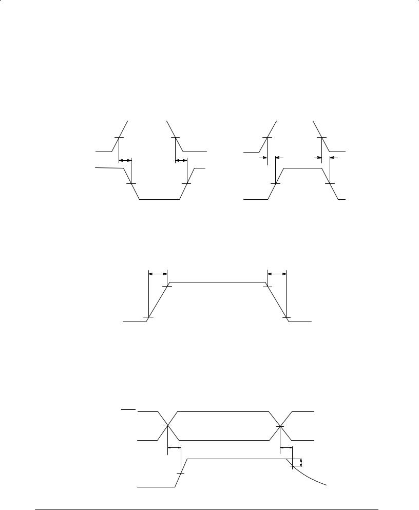
AC SWITCHING PARAMETERS AND WAVEFORMS
tPLH
tPHL
LOW-TO-HIGH propagation delay time :
The time delay between specified reference points, typically 1.3 V for LS and 1.5 V for FAST, on the input and output voltage waveforms, with the output changing from the defined LOW level to the defined HIGH level.
HIGH-TO-LOW propagation delay time:
The time delay between specified reference points, typically 1.3 V for LS and 1.5 V for FAST, on the input and output voltage waveforms, with the output changing from the defined HIGH level to the defined LOW level.
For Inverting Function |
For Non-Inverting |
||||
|
|
|
|
|
|
tr
tf
tPHZ
tPZH
VIN |
tPHL |
VIN |
tPHL |
|
tPLH |
||
Vout |
|
tPLH |
|
Vout
Waveform Rise Time:
LOW to HIGH logic transition time, measured from the 10% to 90% points of the waveform.
Waveform Fall Time:
HIGH to LOW logic transition time, measured the 90% to the 10% points of the waveform.
tr |
tf |
90% |
90% |
10% |
10% |
Output disable time: HIGH to Z
The time delay between the specified reference points on the input and output voltage waveforms, with the 3-state output changing from the defined HIGH level to a high impedance (OFF) state. Reference point on the output voltage waveform is VOH ± 0.5 V for LS and VOH ± 0.3 V for FAST.
Output enable time: Z to HIGH
The time delay between the specified reference points on the input and output voltage waveforms, with the 3-state output changing from a high impedance (OFF) state to a HIGH level.
Enable |
|
|
Enable |
|
tPHZ |
|
|
|
|
tPZH |
VOH ≈ 3.5 V |
|
|
.5 for LS |
|
|
.3 for FAST |
Vout |
|
|
FAST AND LS TTL DATA
3-8
tPLZ
tPZL
trec
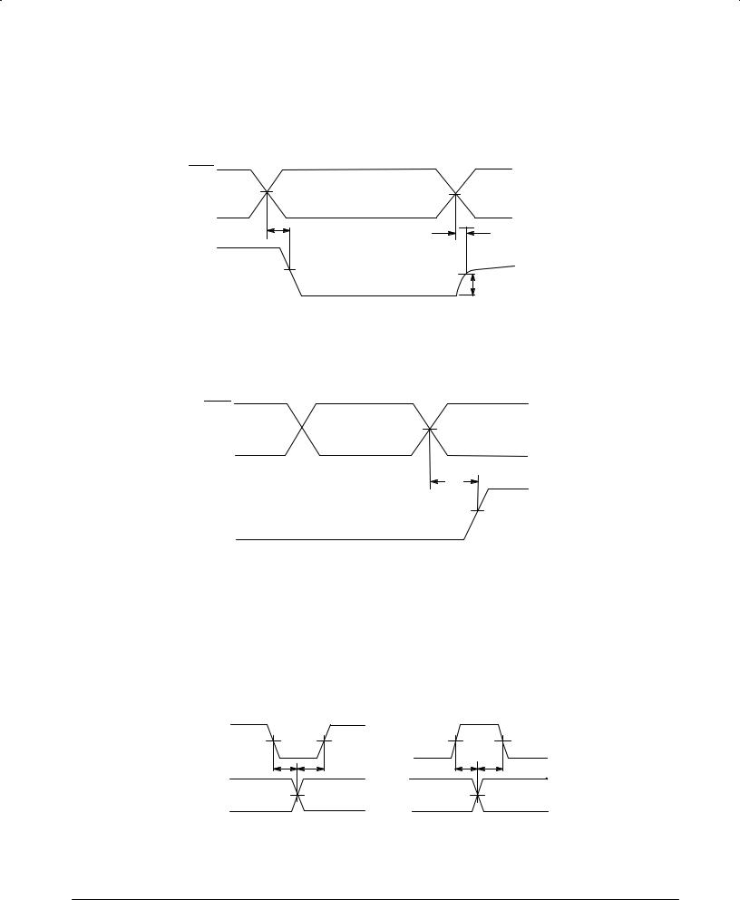
Output disable time: LOW to Z
The time delay between the specified reference points on the input and output voltage waveforms, with the 3-state output changing from the defined LOW level to a high impedance (OFF) state. Reference point on the output voltage waveform is VOL + 0.5 V for LS and VOL + 0.3 V for FAST.
Output enable time: Z to LOW
The time delay between the specified reference points on the input and output voltage waveforms with the 3-state output changing from a high impedance (OFF) state to a HIGH level.
Enable
Enable
tPLZ
tPZL
Vout
VOZ = 1.5 V
.5 for LS
.3 for FAST
Recovery time
Time required between an asynchronous signal (SET, RESET, CLEAR or PARALLEL load) and the active edge of a synchronous control signal, to insure that the device will properly respond to the synchronous signal.
Asynch
Asynch
trec
Control
th
ts
Hold Time
The interval of time from the active edge of the control signal (usually the clock) to when the data to be recognized is no longer required to ensure proper interpretation of the data. A negative hold time indicates that the data may be removed at some time prior to the active edge of the control signal.
Setup time
The interval of time during which the data to be recognized is required to remain constant prior to the active edge of the control signal to ensure proper data recognition. A negative setup time indicates that data may be initiated sometime after the active transition of the timing pulse and still be recognized.
VIN |
|
VIN |
|
ts(L) |
th(L) |
ts(H) |
th(H) |
CP |
|
CP |
|
FAST AND LS TTL DATA
3-9
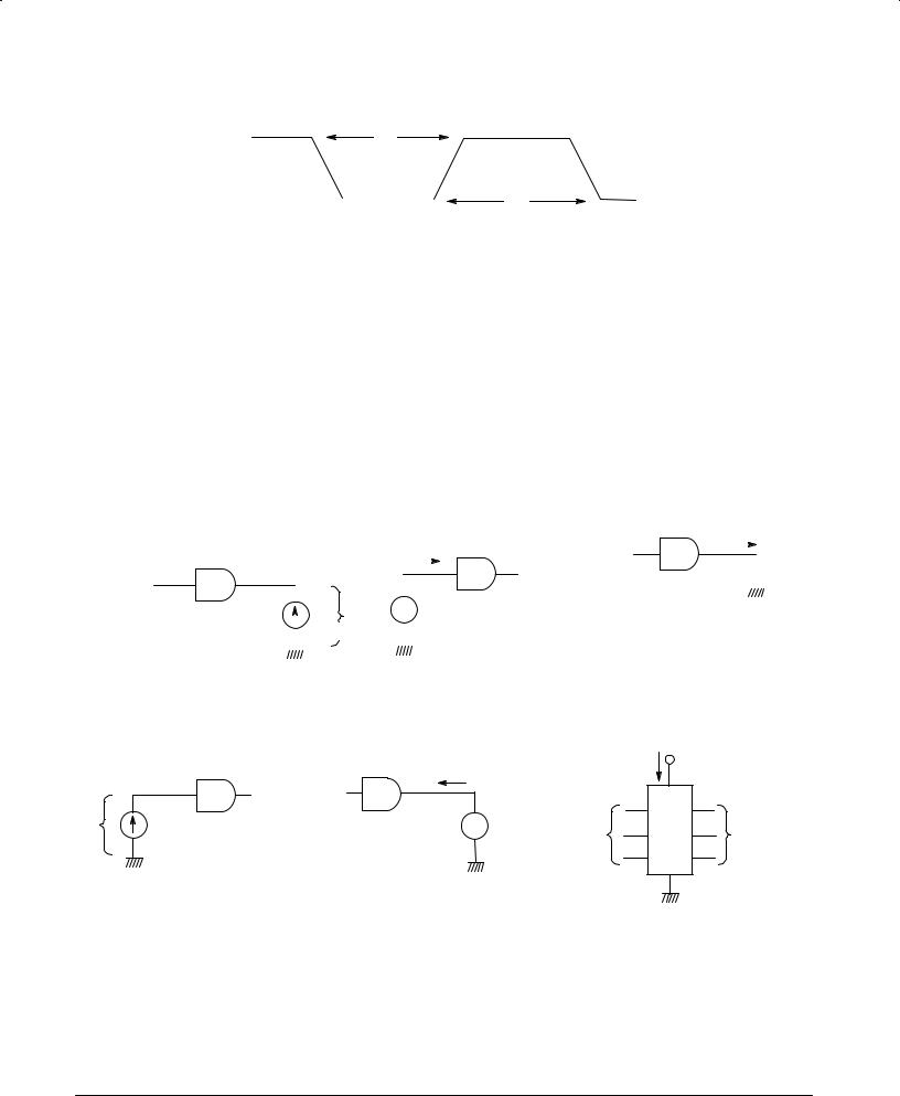
tw or |
Pulse width |
|||||||||||
tpw |
The time between the specified amplitude points (1.3 V for LS and 1.5 V for FAST ) on the leading and trailing |
|||||||||||
|
edges of a pulse. |
|||||||||||
|
|
|
|
|
twL |
|
|
|
||||
|
|
|
|
|
|
|
|
|
|
|
||
|
|
|
|
|
|
|
|
|
|
|
|
|
|
|
|
|
|
|
|
|
|
|
|
|
|
|
|
|
|
|
|
|
|
|
twH |
|
|
|
|
|
|
|
|
|
|
|
|
|
|
||
|
|
|
|
|
|
|
|
|
|
|
||
fMAX
fMAXmin
Toggle frequency/operating frequency
The maximum rate at which clock pulses meeting the clock requirements (ie., tWH, tWL, and tr, tf) may be applied to a sequential circuit. Above this frequency the device may cease to function.
Guaranteed maximum clock frequency
The lowest possible value for fMAX.
TESTING
DC TEST CIRCUITS
The following test circuits and forcing functions represent Motorola's typical DC test procedures.
|
VOH AND VOL TESTS |
|
|
|
|
IIHH, IIH AND IIL TESTS |
|
IOS TEST |
|
||||||||||
|
Force IOHMAX or IOLMAX |
|
|
|
|
Force 7, 5.5, 2.7, or 0.4 V |
|
Measure |
|
||||||||||
|
Measure V |
or V |
|
|
|
|
|
Measure I |
, I |
, or I |
|
|
IOS |
|
|||||
|
OH |
OL |
|
|
|
|
|
|
|
|
IHH |
IH |
IL |
VIHMIN |
|
|
|
|
|
|
|
|
|
|
|
|
|
|
|
|
|
|
|
|
DUT |
|
|||
VIHMIN |
DUT |
|
|
+ |
|
|
|
|
|
|
DUT |
or VILMAX |
|
||||||
|
|
|
|
|
|
|
|
|
|
|
|
||||||||
|
|
|
|
|
|
|
|
|
|
|
|
|
|||||||
or VILMAX |
|
|
|
|
|
|
|
|
|
|
|
|
|
|
|
|
|
|
|
|
Io |
|
|
|
Vi |
|
|
|
|
|
|
|
|||||||
|
|
|
|
|
|
|
|
|
|
|
|
||||||||
|
|
|
|
|
|
|
|
|
|
||||||||||
|
|
|
|
|
Vo |
|
|
|
|
|
|
|
|
|
|
|
|||
|
|
|
|
|
|
|
|
|
|
|
|
|
|
|
|
|
|
|
|
|
|
|
|
|
|
|
|
|
|
|
|
|
|
|
|
|
|
|
|
|
|
|
|
|
|
|
|
|
|
|
|
|
|
|
|
|
|
|
|
|
VIK TEST |
IOH, IOZH, and IOZL TESTS |
|
ICC TEST |
|
|
|
Force Ii |
Force 5.5, 2.4, or 0.4 V |
|
Measure ICC |
VCC MAX |
|
|
Measure VIK |
Measure IO |
|
|
||
|
|
Io |
|
|
|
|
+ |
DUT |
DUT |
|
|
|
|
Vik |
Ii = ±18 mA |
± |
V |
GND |
DUT |
Outputs |
|
|
|
o |
or |
Open |
|
|
|
|
|
|
||
|
|
|
|
4.5 V* |
|
|
± |
|
|
|
|
|
|
|
|
|
|
|
|
|
*Unless otherwise indicated, input conditions are selected to produce a worst case condition.
FAST AND LS TTL DATA
3-10