Материал: 9415

DISCRETE SEMICONDUCTORS
PHN110
N-channel enhancement mode MOS transistor
Product specification |
1996 Apr 02 |
Supersedes data of November 1994
File under Discrete Semiconductors, SC07
Philips Semiconductors |
Product specification |
|
|
|
|
N-channel enhancement mode
PHN110
MOS transistor
FEATURES
∙High speed switching
∙No secondary breakdown
∙Very low on-resistance.
DESCRIPTION
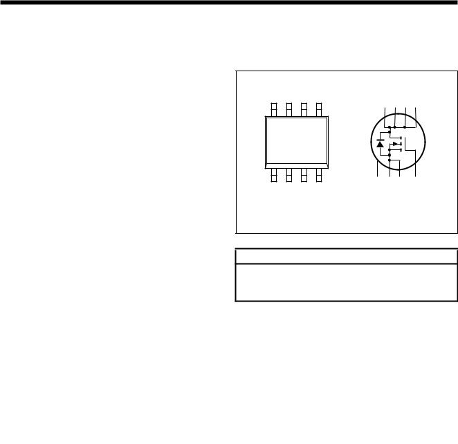
N-channel enhancement mode MOS transistor in an 8-pin plastic SO8 (SOT96-1) package.
APPLICATIONS
∙Motor and actuator driver
∙Power management
∙Synchronized rectifying.
PINNING - SO8 (SOT96-1)
PIN |
SYMBOL |
DESCRIPTION |
|
|
|
1 |
n.c |
not connected |
2 |
s |
source |
3 |
s |
source |
4 |
g |
gate |
5 |
d |
drain |
6 |
d |
drain |
7 |
d |
drain |
8 |
d |
drain |
|
|
|
handbook, halfpage |
|
d |
d d |
d |
8 |
5 |
|
|
|
1 |
4 |
|
|
|
|
MAM116 |
n.c. s |
s |
g |
Fig.1 Simplified outline and symbol.
CAUTION
The device is supplied in an antistatic package. The gate-source input must be protected against static discharge during transport or handling.
QUICK REFERENCE DATA
SYMBOL |
PARAMETER |
CONDITIONS |
|
MIN. |
MAX. |
UNIT |
|
|
|
|
|
|
|
VDS |
drain-source voltage (DC) |
|
− |
|
30 |
V |
VSD |
source-drain diode forward voltage |
IS = 1.25 A |
− |
|
1.2 |
V |
VGS |
gate-source voltage (DC) |
|
− |
|
±20 |
V |
VGSth |
gate-source threshold voltage |
ID = 1 mA; VDS = VGS |
1 |
|
2.8 |
V |
ID |
drain current (DC) |
Ts = 80 °C |
− |
|
4 |
A |
RDSon |
drain-source on-state resistance |
ID = 2.2 A; VGS = 10 V |
− |
|
0.1 |
Ω |
Ptot |
total power dissipation |
Ts = 80 °C |
− |
|
2.8 |
W |
1996 Apr 02 |
2 |
Philips Semiconductors |
Product specification |
|
|
N-channel enhancement mode
PHN110
MOS transistor
LIMITING VALUES
In accordance with the Absolute Maximum Rating System (IEC 134).
SYMBOL |
PARAMETER |
CONDITIONS |
MIN. |
MAX. |
UNIT |
|
|
|
|
|
|
|
|
VDS |
drain-source voltage (DC) |
|
− |
30 |
V |
|
VGS |
gate-source voltage (DC) |
|
− |
±20 |
V |
|
ID |
drain current (DC) |
Ts = 80 °C; note 1 |
− |
4 |
A |
|
IDM |
peak drain current |
note 2 |
− |
16 |
A |
|
Ptot |
total power dissipation |
Ts = 80 °C |
− |
2.8 |
W |
|
|
|
|
Tamb = 25 °C; note 3 |
− |
2.4 |
W |
|
|
|
Tamb = 25 °C; note 4 |
− |
1.1 |
W |
Tstg |
storage temperature |
|
−65 |
+150 |
°C |
|
Tj |
operating junction temperature |
|
−65 |
+150 |
°C |
|
Source-drain diode |
|
|
|
|
||
|
|
|
|
|
|
|
IS |
source current (DC) |
Ts = 80 °C |
− |
3.5 |
A |
|
ISM |
peak pulsed source current |
note 2 |
− |
14 |
A |
|
Notes
1.Ts is the temperature at the soldering point of the drain lead.
2.Pulse width and duty cycle limited by maximum junction temperature.
3.Value based on PCB with a Rth a-tp (ambient to tie-point) of 27.5 K/W.
4.Value based on PCB with a Rth a-tp (ambient to tie-point) of 90 K/W.
6 |
|
|
|
|
MBG848 |
102 |
|
|
MBG750 |
|
|
|
|
|
|
|
|
|
|
||
handbook, halfpage |
|
|
|
|
|
handbook, halfpage |
|
|
|
|
Ptot |
|
|
|
|
|
ID |
|
|
|
|
|
|
|
|
|
(A) |
|
|
|
|
|
(W) |
|
|
|
|
|
10 |
|
|
|
|
|
|
|
|
|
|
|
|
tp = |
|
|
|
|
|
|
|
|
(1) |
|
|
|
|
4 |
|
|
|
|
|
|
|
|
10 μs |
|
|
|
|
|
|
|
|
|
|
100 μs |
|
|
|
|
|
|
|
1 |
|
|
1 ms |
|
|
|
|
|
|
|
P |
t p |
|
10 ms |
|
2 |
|
|
|
|
|
δ = |
|
|
|
|
|
|
|
|
|
|
T |
DC |
100 ms |
||
|
|
|
|
|
|
10−1 |
|
|||
|
|
|
|
|
|
|
|
|
||
|
|
|
|
|
|
|
|
|
|
|
|
|
|
|
|
|
t p |
t |
|
|
|
|
|
|
|
|
|
T |
|
|
|
|
0 |
|
|
|
|
|
10−2 |
|
|
|
102 |
0 |
50 |
100 |
150 T |
s |
(oC) 200 |
10−1 |
1 |
10 |
VDS (V) |
|
|
|
|
|
|||||||
|
|
|
|
|
|
|
|
|
|
|
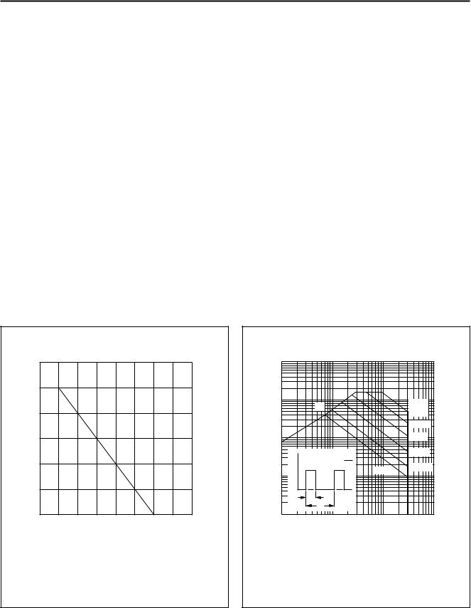
δ = 0.01; TS = 80 °C.
(1) RDSon limitation.
Fig.2 Power derating curve. |
Fig.3 DC SOAR. |
1996 Apr 02 |
3 |
Philips Semiconductors |
Product specification |
|
|
N-channel enhancement mode
PHN110
MOS transistor
THERMAL CHARACTERISTICS
SYMBOL |
PARAMETER |
VALUE |
UNIT |
|
|
|
|
Rth j-s |
thermal resistance from junction to soldering point |
25 |
K/W |
102 |
|
|
|
|
|
MBG749 |
|
|
|
|
|
|
|
|
|
handbook, full pagewidth |
|
|
|
|
|
|
|
Rth j−s |
|
|
|
|
|
|
|
(K/W) |
δ = |
|
|
|
|
|
|
|
|
|
|
|
|
|
|
|
0.75 |
|
|
|
|
|
|
10 |
0.5 |
|
|
|
|
|
|
0.33 |
|
|
|
|
|
|
|
|
|
|
|
|
|
|
|
|
0.2 |
|
|
|
|
|
|
|
0.1 |
|
|
|
|
|
|
|
0.05 |
|
|
|
|
|
|
1 |
0.02 |
|
|
|
P |
t p |
|
|
|
|
|
δ = |
|
||
|
|
|
|
|
|
T |
|
|
0.01 |
|
|
|
|
|
|
|
0 |
|
|
|
t p |
t |
|
|
|
|
|
|
|
||
|
|
|
|
|
|
T |
|
10−1 |
|
|
|
|
|
|
|
10−6 |
10−5 |
10−4 |
10−3 |
10−2 |
10−1 |
tp (s) |
1 |
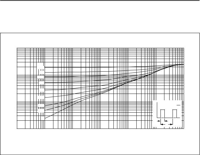
Fig.4 Transient thermal resistance from junction to soldering point as a function of pulse time; typical values
1996 Apr 02 |
4 |

Philips Semiconductors |
Product specification |
|
|
N-channel enhancement mode
PHN110
MOS transistor
CHARACTERISTICS
Tj = 25 °C unless otherwise specified.
SYMBOL |
PARAMETER |
CONDITIONS |
MIN. |
TYP. |
MAX. |
UNIT |
|
|
|
|
|
|
|
V(BR)DSS |
drain-source breakdown voltage |
VGS = 0; ID = 10 μA |
30 |
− |
− |
V |
VGSth |
gate-source threshold voltage |
VGS = VDS; ID = 1 mA |
1 |
− |
2.8 |
V |
IDSS |
drain-source leakage current |
VGS = 0; VDS = 24 V |
− |
− |
100 |
nA |
IGSS |
gate leakage current |
VGS = ±20 V; VDS = 0 |
− |
− |
±100 |
nA |
RDSon |
drain-source on-state resistance |
VGS = 4.5 V; ID = 1 A |
− |
0.11 |
0.2 |
Ω |
|
|
VGS = 10 V; ID = 2 A |
− |
0.08 |
0.1 |
Ω |
Ciss |
input capacitance |
VGS = 0; VDS = 24 V; f = 1 MHz |
− |
250 |
− |
pF |
Coss |
output capacitance |
VGS = 0; VDS = 24 V; f = 1 MHz |
− |
140 |
− |
pF |
Crss |
reverse transfer capacitance |
VGS = 0; VDS = 24 V; f = 1 MHz |
− |
50 |
− |
pF |
Qg |
total gate charge |
VGS = 10 V; VDD = 15 V; ID = 2 A |
− |
10 |
30 |
nC |
Qgs |
gate-source charge |
VGS = 10 V; VDD = 15 V; ID = 2 A |
− |
1 |
− |
nC |
Qgd |
gate-drain charge |
VGS = 10 V; VDD = 15 V; ID = 2 A |
− |
2.5 |
− |
nC |
Switching times (see Fig 11) |
|
|
|
|
|
|
|
|
|
|
|
|
|
td(on) |
turn-on delay time |
VGS = 0 to 10 V; VDD = 15 V; |
− |
4.5 |
− |
ns |
|
|
ID = 1 A; RL = 15 Ω; Rgen = 6 Ω |
|
|
|
|
tf |
fall time |
− |
3.5 |
− |
ns |
|
ton |
turn-on switching time |
|
− |
8 |
16 |
ns |
td(off) |
turn-off delay time |
VGS = 10 to 0 V; VDD = 15 V; |
− |
15 |
− |
ns |
|
|
ID = 1 A; RL = 15 Ω; Rgen = 6 Ω |
|
|
|
|
tr |
rise time |
− |
10 |
− |
ns |
|
toff |
turn-off switching time |
|
− |
25 |
50 |
ns |
Source-drain diode |
|
|
|
|
|
|
|
|
|
|
|
|
|
VSD |
source-drain diode forward voltage |
VGS = 0; IS = 1.25 A |
− |
− |
1.2 |
V |
trr |
reverse recovery time |
IS = 1.25 A; di/dt = −100 A/μs |
− |
35 |
100 |
ns |
1996 Apr 02 |
5 |