Материал: TC7106
TC7106
TC7106A
TC7107
TC7107A
3-1/2 DIGIT A/D CONVERTERS
FEATURES |
GENERAL DESCRIPTION |
1
2
■ Internal Reference with Low Temperature Drift |
|
TC7106/7 ....................................... |
80ppm/°C Typical |
TC7106A/7A .................................. |
20ppm/°C Typical |
■Drives LCD (TC7106) or LED (TC7107) Display Directly
■Guaranteed Zero Reading With Zero Input
■Low Noise for Stable Display
■Auto-Zero Cycle Eliminates Need for Zero Adjustment
■True Polarity Indication for Precision Null Applications
■Convenient 9 V Battery Operation (TC7106A)
■ High Impedance CMOS Differential Inputs .... 1012Ω
■Differential Reference Inputs Simplify Ratiometric Measurements
■ Low Power Operation |
..................................... 10mW |
ORDERING INFORMATION |
|
|
|
PART CODE |
TC710X X X XXX |
6 = LCD }
7 = LED
A or blank*
R (reversed pins) or blank (CPL pkg only)
* "A" parts have an improved reference TC
Package Code (see below):
Package |
|
|
Temperature |
Code |
Package |
Pin Layout |
Range |
|
|
|
|
CKW |
44-Pin PQFP |
Formed Leads |
0°C to +70°C |
|
|
|
|
CLW |
44-Pin PLCC |
— |
0°C to +70°C |
|
|
|
|
CPL |
40-Pin PDIP |
Normal |
0°C to +70°C |
|
|
|
|
IPL |
40-Pin PDIP |
Normal |
– 25°C to +85°C |
|
|
|
|
IJL |
40-Pin CerDIP |
Normal |
– 25°C to +85°C |
|
|
|
|
AVAILABLE PACKAGES
40-Pin Plastic DIP |
40-Pin CERDIP |
44-Pin Plastic Quad Flat |
44-Pin Plastic Chip |
Package Formed Leads |
Carrier PLCC |
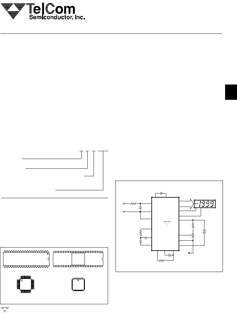
The TC7106A and TC7107A 3-1/2 digit direct-display |
|
drive analog-to-digital converters allow existing 7106/7107 |
|
based systems to be upgraded. Each device has a preci- |
|
sion reference with a 20ppm/°C max temperature coeffi- |
|
cient. This represents a 4 to 7 times improvement over |
|
similar 3-1/2 digit converters. Existing 7106 and 7107 based |
3 |
systems may be upgraded without changing external pas- |
|
sive component values. The TC7107A drives common |
|
anode light emitting diode (LED) displays directly with 8mA |
|
per segment. A low-cost, high-resolution indicating meter |
|
requires only a display, four resistors, and four capacitors. |
|
The TC7106A low power drain and 9V battery operation |
|
make it suitable for portable applications. |
4 |
The TC7106A/TC7107A reduces linearity error to less |
|
than 1 count. Rollover error – the difference in readings for |
|
equal magnitude but opposite polarity input signals – is |
below ±1 count. High impedance differential inputs offer 1pA leakage current and a 1012Ω input impedance. The differential reference input allows ratiometric measurements for ohms or bridge transducer measurements. The 15μVP–P noise performance guarantees a “rock solid” reading. The auto-zero cycle guarantees a zero display read-
ing with a zero-volts input. |
5 |
|
|
|
|
0.1 F |
|
|
|
|
|
|
|
||
|
|
|
34 |
|
33 |
|
|
|
LCD DISPLAY (TC7106/A) OR |
|
||
|
|
|
|
|
|
|
|
COMMON ANODE LED |
|
|||
|
1MΩ |
31 |
CREF+ |
|
CREF– |
|
SEGMENT |
DISPLAY (TC7107/A) |
|
|||
+ |
|
V+ |
|
|
|
2–19 |
|
|
|
|||
|
|
|
|
|
|
|
|
|||||
ANALOG |
0.01 F |
|
IN |
|
|
|
22–25 |
DRIVE |
|
|
6 |
|
|
|
|
|
|
|
|
|
|
|
|||
INPUT |
|
VIN– |
|
|
|
|
20 |
|
|
|
||
|
30 |
|
|
|
POL |
|
|
|
||||
– |
|
|
|
|
MINUS SIGN |
BACKPLANE |
||||||
|
|
|
|
|
|
|
|
21 |
||||
|
|
32 |
ANALOG |
|
BP |
|
|
DRIVE |
||||
|
|
|
1 |
|
|
|
||||||
|
|
COMMON |
|
V+ |
|
|
|
|||||
|
|
28 |
|
|
TC7106/A |
|
|
24kΩ |
|
|
||
|
|
V |
|
|
|
|
+ |
|
||||
|
47kΩ |
|
BUFF |
|
TC7107/A |
36 |
VREF |
1kΩ |
9V |
|
||
|
0.47 F |
|
|
|
|
+ |
|
|
||||
|
|
CAZ |
|
|
|
VREF |
|
|
|
|
|
|
|
|
29 |
|
|
|
V–REF |
35 |
100mV |
|
|
|
|
|
0.22 F |
|
|
|
|
|
|
|
||||
|
|
27 |
VINT |
|
|
|
V– |
26 |
|
|
|
|
|
|
|
|
|
|
|
|
|
|
|||
|
|
|
OSC2 |
OSC3 |
OSC1 |
|
|
TO ANALOG |
7 |
|||
|
|
|
39 |
|
38 |
COSC 40 |
|
|
||||
|
|
|
|
|
|
COMMON (PIN 32) |
||||||
|
|
|
R |
OSC |
100pF |
3 CONVERSIONS/SEC |
||||||
|
|
|
|
|
|
200mV FULL SCALE |
||||||
|
|
|
100kΩ |
|
|
|
|
|
|
|
||
Figure 1. TC7106/A/7/A Typical Operating Circuit
8
TC7106/6A/7/7A-7 11/4/96
TELCOM SEMICONDUCTOR, INC. |
3-183 |

3-1/2 DIGIT A/D CONVERTERS
TC7106
TC7106A
TC7107
TC7107A
ABSOLUTE MAXIMUM RATINGS*
TC7106A
Supply Voltage (V+ to V–) ........................................... |
|
15 V |
Analog Input Voltage (either input) (Note 1) |
......... V+ to V– |
|
Reference Input Voltage (either input) ................. |
|
V+ to V– |
Clock Input ........................................................ |
|
Test to V+ |
Package Power Dissipation (Note 2) (TA ≤ 70°C) |
||
CerDIP .............................................................. |
|
2.29W |
Plastic DIP ........................................................ |
|
1.23W |
PLCC ................................................................ |
|
1.23W |
PQFP ................................................................ |
|
1.00W |
Operating Temperature |
|
0 ° C to +70°C |
“C” Devices ............................................ |
|
|
“I” Devices ........................................ |
– 25°C to +85°C |
|
Storage Temperature ............................ |
– 65°C to +150°C |
|
Lead Temperature (Soldering, 60 sec) ................... |
|
300°C |
TC7107A
Supply Voltage
V+ ................................................................................................ |
+6 V |
V– ............................................................................................... |
– 9 V |
Analog Input Voltage (either input) (Note 1) |
......... V+ to V– |
|
Reference Input Voltage (either input) ................. |
|
V+ to V– |
Clock Input ....................................................... |
|
GND to V+ |
Power Dissipation (Note 2) (TA ≤ 70°C) |
|
|
40-Pin CerDIP Package ................................... |
|
2.29W |
40-Pin Plastic DIP ............................................. |
|
1.23W |
44-Pin PLCC ..................................................... |
|
1.23W |
44-Pin PQFP .................................................... |
|
1.00W |
Operating Temperature |
|
0 ° C to +70°C |
“C” Devices ............................................ |
|
|
“I” Devices ........................................ |
– 25°C to +85°C |
|
Storage Temperature ............................ |
– 65°C to +150°C |
|
Lead Temperature (Soldering, 10 sec) ................. |
|
+300°C |
|
|
|
*Static-sensitive device. Unused devices must be stored in conductive material. Protect devices from static discharge and static fields. Stresses above those listed under Absolute Maximum Ratings may cause permanent damage to the device. These are stress ratings only and functional operation of the device at these or any other conditions above those indicated in the operational sections of the specifications is not implied. Exposure to Absolute Maximum Rating Conditions for extended periods may affect device reliability.
ELECTRICAL CHARACTERISTICS (Note 3)
Parameters |
Test Conditions |
TC7106/A & TC7107/A |
Unit |
||
Min |
Typ |
Max |
|||
|
|
|
|
|
|
Zero Input Reading |
VIN = 0.0 V |
– 000.0 |
±000.0 |
+000.0 |
Digital |
|
Full-Scale = 200.0mV |
|
|
|
Reading |
|
|
|
|
|
|
Ratiometric Reading |
VIN = VREF |
999 |
999/1000 |
1000 |
Digital |
|
VREF = 100 mV |
|
|
|
Reading |
Roll-Over Error (Difference in |
VIN– = +VIN+ 200mV |
– 1 |
±0.2 |
+1 |
Counts |
Reading for Equal Positive and |
|
|
|
|
|
Negative Reading Near Full-Scale) |
|
|
|
|
|
|
|
|
|
|
|
Linearity (Max. Deviation From |
Full-Scale = 200mV |
– 1 |
±0.2 |
+1 |
Counts |
Best Straight Line Fit) |
or Full-Scale = 2.000 V |
|
|
|
|
|
|
|
|
|
|
Common-Mode |
VCM = ±1V, VIN = 0V, |
— |
50 |
— |
μV/V |
Rejection Ratio (Note 4) |
Full Scale = 200.0 mV |
|
|
|
|
|
|
|
|
|
|
Noise (Pk – Pk Value Not |
VIN = 0 V |
— |
15 |
— |
μV |
Exceeded 95% of Time) |
Full-Scale = 200.0mV |
|
|
|
|
|
|
|
|
|
|
Leakage Current @ Input |
VIN = 0 V |
— |
1 |
10 |
pA |
Zero Reading Drift |
VIN = 0 V |
|
|
|
|
|
“C” Device = 0°C to +70°C |
— |
0.2 |
1 |
μV/°C |
|
VIN = 0 V |
|
|
|
|
|
“I” Device = – 25°C to +85°C |
— |
1.0 |
2 |
μV/°C |
|
|
|
|
|
|
Scale Factor |
VIN = 199.0mV, |
|
|
|
|
Temperature Coefficient |
“C” Device = 0°C to +70°C |
— |
1 |
5 |
ppm/°C |
|
(Ext. Ref = 0ppm°C) |
|
|
|
ppm/°C |
|
VIN = 199.0mV |
— |
— |
20 |
|
|
“I” Device = – 25°C to +85°C |
|
|
|
|
|
|
|
|
|
|
Supply Current (Does Not |
VIN = 0 |
— |
0.8 |
1.8 |
mA |
Include LED Current For TC7107/A) |
|
|
|
|
|
|
|
|
|
|
|
3-184 |
TELCOM SEMICONDUCTOR, INC. |

3-1/2 DIGIT A/D CONVERTERS
TC7106 1 TC7106A
TC7107
TC7107A
ELECTRICAL CHARACTERISTICS (Cont.) (Note 3)
Parameters |
Test Conditions |
TC7106/A & TC7107/A |
Unit |
||
Min |
Typ |
Max |
|||
|
|
|
|
|
|
Analog Common Voltage |
25kΩ Between Common |
2.7 |
3.05 |
3.35 |
V |
(With Respect to Pos. Supply) |
and Pos. Supply |
|
|
|
|
|
|
|
|
|
|
Temp. Coeff. of |
25kΩ Between Common |
|
|
|
|
Analog Common |
and Pos. Supply |
|
|
|
|
(With Respect |
0°C ≤ TA ≤ +70°C |
7106A/7A |
20 |
50 |
ppm/°C |
to Pos. Supply) |
("C", Commercial Temp. Range Devices) |
7106/7 |
80 |
— |
ppm/°C |
|
|
|
|
|
|
Temp. Coeff. of |
25kΩ Between Common |
|
|
|
|
Analog Common |
and Pos. Supply |
|
|
|
|
(With Respect |
– 25°C ≤ TA ≤ 85°C |
— |
— |
75 |
ppm/°C |
to Pos. Supply) |
(“I,” Industrial Temp. Range Devices) |
|
|
|
|
|
|
|
|
|
|
TC7106A ONLY Pk – Pk |
V+ to V– = 9V |
4 |
5 |
6 |
V |
Segment Drive Voltage (Note 5) |
|
|
|
|
|
|
|
|
|
|
|
TC7106A ONLY Pk – Pk |
V+ to V– = 9V |
4 |
5 |
6 |
V |
Backplane Drive Voltage (Note 5) |
|
|
|
|
|
|
|
|
|
|
|
TC7107A ONLY |
V+ = 5.0V |
5 |
8.0 |
— |
mA |
Segment Sinking Current (Except Pin 19) |
Segment Voltage = 3V |
|
|
|
|
|
|
|
|
|
|
TC7107A ONLY |
V+ = 5.0V |
10 |
16 |
— |
mA |
Segment Sinking Current (Pin 19) |
Segment Voltage = 3V |
|
|
|
|
|
|
|
|
|
|
NOTES: 1. Input voltages may exceed the supply voltages provided the input current is limited to ±100μA.
2.Dissipation rating assumes device is mounted with all leads soldered to printed circuit board.
3.Unless otherwise noted, specifications apply to both the TC7106/A and TC7107/A at TA = 25°C, fCLOCK = 48 kHz. Parts are tested in the circuit of Figure 1.
4. Refer to “Differential Input” discussion.
5.Backplane drive is in phase with segment drive for “OFF” segment, 180° out of phase for “ON” segment. Frequency is 20 times conversion rate. Average DC component is less than 50mV.
2
3
4
5
6
7
8
TELCOM SEMICONDUCTOR, INC. |
3-185 |
3-1/2 DIGIT A/D CONVERTERS
TC7106
TC7106A
TC7107
TC7107A
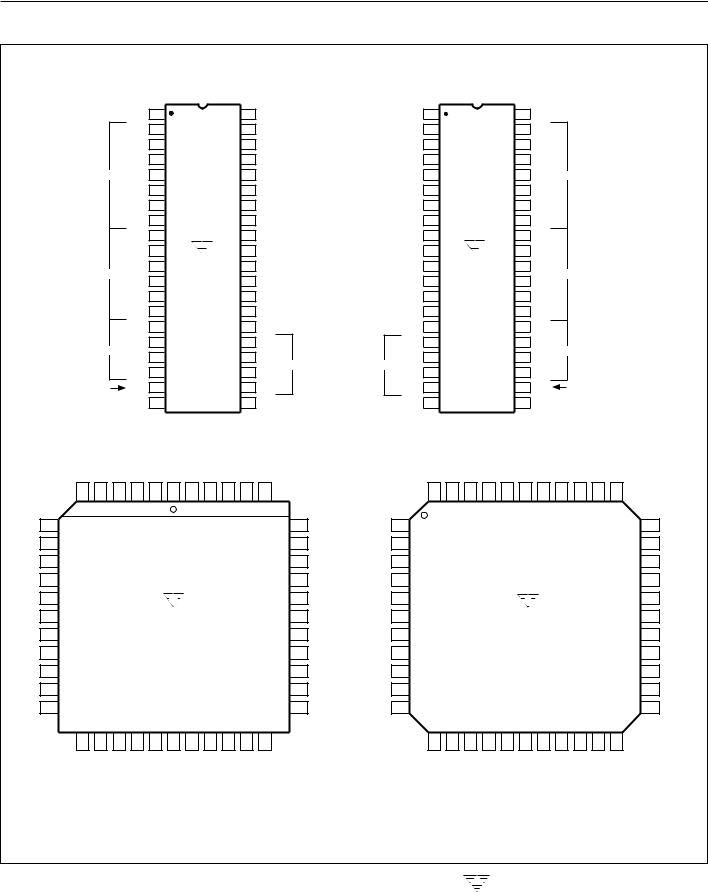
PIN CONFIGURATIONS
|
|
|
|
|
V+ |
1 |
NORMAL PIN |
40 |
OSC 1 |
|
|
|
|
OSC1 |
1 |
REVERSE PIN |
40 |
V+ |
|
|
|
|
|
|
||||||
|
|
|
|
|
D1 |
2 |
39 |
OSC2 |
|
|
|
|
OSC2 |
2 |
39 |
D1 |
|
|
|
|
|
|
||||||||
|
|
|
|
|
CONFIGURATION |
|
|
|
|
CONFIGURATION |
|
|
|
|
|
|
||||||||||||||
|
|
|
|
|
C1 |
3 |
|
|
|
|
38 |
OSC 3 |
|
|
|
|
OSC 3 |
3 |
|
|
|
|
38 |
C1 |
|
|
|
|
|
|
|
|
|
|
|
B1 |
4 |
|
|
|
|
37 |
TEST |
|
|
|
|
TEST |
4 |
|
|
|
|
37 |
B1 |
|
|
|
|
|
|
|
|
|
|
|
A1 |
|
|
|
|
|
|
+ |
|
|
|
|
+ |
|
|
|
|
|
|
A1 |
|
|
|
|
|
|
|
|
|
1's |
5 |
|
|
|
|
36 |
VREF |
|
|
|
|
VREF |
5 |
|
|
|
|
36 |
1's |
|
|
|
|
||||
|
|
|
|
|
F1 |
|
|
|
|
|
|
– |
|
|
|
|
– |
|
|
|
|
|
|
F1 |
|
|
|
|
|
|
|
|
|
|
|
6 |
|
|
|
|
35 |
VREF |
|
|
|
|
VREF |
6 |
|
|
|
|
35 |
|
|
|
|
|
|
||
|
|
|
|
|
G |
7 |
|
|
|
|
34 |
+ |
|
|
|
|
C+ |
7 |
|
|
|
|
34 |
G |
|
|
|
|
|
|
|
|
|
|
|
1 |
|
|
|
|
CREF |
|
|
|
|
REF |
|
|
|
|
1 |
|
|
|
|
|
|
||||
|
|
|
|
|
E1 |
|
|
|
|
|
|
– |
|
|
|
|
– |
|
|
|
|
|
|
E1 |
|
|
|
|
|
|
|
|
|
|
|
8 |
|
|
|
|
33 |
CREF |
|
|
|
|
CREF |
8 |
|
|
|
|
33 |
|
|
|
|
|
|
||
|
|
|
|
|
D2 |
9 |
|
|
|
|
32 |
ANALOG |
|
|
|
ANALOG |
9 |
|
|
|
|
32 |
D2 |
|
|
|
|
|
|
|
|
|
|
|
|
|
|
|
|
COMMON |
|
|
COMMON |
|
|
|
|
|
|
|
|
|
|
||||||||
|
|
|
|
|
C2 |
10 |
|
|
|
|
31 |
+ |
|
|
|
|
+ |
10 |
|
|
|
|
31 |
C2 |
|
|
|
|
|
|
|
|
|
|
|
|
|
|
|
VIN |
|
|
|
|
VIN |
|
|
|
|
|
|
|
|
|
|
||||||
|
|
|
|
|
B2 |
11 |
TC7106ACPL |
30 |
– |
|
|
|
|
V – |
11 |
TC7106AIJL |
30 |
B2 |
|
|
|
|
|
|
||||||
|
|
|
10's |
TC7107AIPL |
V IN |
|
|
|
|
IN |
TC7107AIJL |
10's |
|
|
|
|
||||||||||||||
|
|
|
A2 |
12 |
29 |
CAZ |
|
|
|
|
CAZ |
12 |
29 |
A2 |
|
|
|
|
||||||||||||
|
|
|
|
|
|
|
|
|
|
|
|
|
|
|
|
|
|
|
|
|
|
|
||||||||
|
|
|
|
|
F2 |
13 |
|
|
|
|
28 |
VBUFF |
|
|
|
VBUFF |
13 |
|
|
|
|
28 |
F2 |
|
|
|
|
|
|
|
|
|
|
|
|
E2 |
14 |
|
|
|
|
27 |
VINT |
|
|
|
|
VINT |
14 |
|
|
|
|
27 |
E2 |
|
|
|
|
|
|
|
|
|
|
|
D3 |
15 |
|
|
|
|
26 |
V – |
|
|
|
|
V – |
15 |
|
|
|
|
26 |
D3 |
|
|
|
|
|
|
|
|
|
100's |
B3 |
16 |
|
|
|
|
25 |
G2 |
|
|
|
|
G2 |
16 |
|
|
|
|
25 |
B3 |
100's |
|
|
|
|
||
|
|
|
F3 |
17 |
|
|
|
|
24 |
C3 |
|
|
|
|
C3 |
17 |
|
|
|
|
24 |
F3 |
|
|
|
|
||||
|
|
|
|
|
|
|
|
|
100's |
|
|
|
|
|
|
|
|
|
|
|
|
|
||||||||
|
|
|
|
|
|
|
|
|
|
|
|
|
|
100's |
|
|
|
|
|
|
|
|
|
|
|
|
|
|||
|
|
|
|
|
E3 |
18 |
|
|
|
|
23 |
A 3 |
|
|
|
|
A 3 |
18 |
|
|
|
|
23 |
E3 |
|
|
|
|
|
|
|
|
1000's |
|
AB 4 |
19 |
|
|
|
|
22 |
G3 |
|
|
|
|
G3 |
19 |
|
|
|
|
22 |
AB4 |
|
1000's |
|
|
|
||
|
|
|
|
|
POL |
20 |
|
|
|
|
21 |
BP/GND |
|
|
|
BP/GND |
20 |
|
|
|
|
21 |
POL |
|
|
|
|
|
|
|
|
|
|
(MINUS SIGN) |
|
|
|
|
|
|
(7106A/7107A) |
|
(7106A/7107A) |
|
|
|
|
|
|
(MINUS SIGN) |
|
|
|
|
|||||||
|
|
1 |
1 |
1 |
1 |
+ |
NC |
1 |
2 |
3 |
TEST |
REF HI |
|
|
|
|
|
REF HI |
REF LO |
REF |
REF |
COM |
IN HI |
IN LO |
A/Z |
BUFF |
INT |
– |
|
|
|
|
A |
B |
C |
D |
V |
OSC |
OSC |
OSC |
|
|
|
|
|
C |
C |
V |
|
|
|||||||||||
|
|
6 |
5 |
4 |
3 |
2 |
1 |
44 |
43 |
42 |
41 |
40 |
|
|
|
|
|
44 |
43 |
42 |
41 |
40 |
39 |
38 |
37 |
36 |
35 |
34 |
|
|
F1 |
7 |
|
|
|
|
|
|
|
|
|
|
39 |
REF LO |
NC |
1 |
|
|
|
|
|
|
|
|
|
|
33 |
NC |
|||
G1 |
8 |
|
|
|
|
|
|
|
|
|
|
38 |
CREF |
NC |
2 |
|
|
|
|
|
|
|
|
|
|
32 |
G2 |
|||
E1 |
9 |
|
|
|
|
|
|
|
|
|
|
37 |
CREF |
TEST |
3 |
|
|
|
|
|
|
|
|
|
|
31 |
C3 |
|||
D2 |
10 |
|
|
|
|
|
|
|
|
|
|
36 |
COMMON |
OSC3 |
4 |
|
|
|
|
|
|
|
|
|
|
30 |
A3 |
|||
C2 |
11 |
|
|
|
|
|
|
|
|
|
|
35 |
IN HI |
NC |
5 |
|
|
|
|
|
|
|
|
|
|
29 |
G3 |
|||
NC |
12 |
|
|
|
TC7106ACLW |
|
|
|
|
34 |
NC |
OSC2 |
6 |
|
|
|
|
TC7106ACKW |
|
|
|
28 |
BP/GND |
|||||||
B2 |
13 |
|
|
|
TC7107ACLW |
|
|
|
|
33 |
IN LO |
OSC1 |
7 |
|
|
|
|
TC7107ACKW |
|
|
|
27 |
POL |
|||||||
|
|
|
(PLCC) |
|
|
|
|
|
|
|
(FLAT PACKAGE) |
|
|
|||||||||||||||||
|
|
|
|
|
|
|
|
|
|
|
|
|
|
|
|
|
|
|
|
|
|
|
||||||||
A2 |
14 |
|
|
|
|
|
|
|
|
|
|
32 |
A/Z |
V+ |
8 |
|
|
|
|
|
|
|
|
|
|
26 |
AB4 |
|||
F2 |
15 |
|
|
|
|
|
|
|
|
|
|
31 |
BUFF |
D1 |
9 |
|
|
|
|
|
|
|
|
|
|
25 |
E3 |
|||
E2 |
16 |
|
|
|
|
|
|
|
|
|
|
30 |
INT |
C1 |
10 |
|
|
|
|
|
|
|
|
|
|
24 |
F3 |
|||
D |
3 |
17 |
|
|
|
|
|
|
|
|
|
|
29 |
V– |
B |
1 |
11 |
|
|
|
|
|
|
|
|
|
|
23 |
B |
3 |
|
|
|
|
|
|
|
|
|
|
|
|
|
|
|
|
|
|
|
|
|
|
|
|
|
|
|
|
|||
|
|
18 |
19 |
20 |
21 |
22 |
23 |
24 |
25 |
26 |
27 |
28 |
|
|
|
|
|
12 |
13 |
14 |
15 |
16 |
17 |
18 |
19 |
20 |
21 |
22 |
|
|
|
|
3 |
3 |
3 |
4 |
POL |
NC |
BP/GND |
3 |
3 |
3 |
2 |
|
|
|
|
|
1 |
1 |
1 |
1 |
2 |
2 |
2 |
2 |
2 |
2 |
3 |
|
|
|
|
B |
F |
E |
AB |
G |
A |
C |
G |
|
|
|
|
|
A |
F |
G |
E |
D |
C |
B |
A |
F |
E |
D |
|
|
|||
3-186 |
TELCOM SEMICONDUCTOR, INC. |

3-1/2 DIGIT A/D CONVERTERS
TC7106
TC7106A
TC7107
TC7107A
PIN DESCRIPTION
Pin No. |
Pin No. |
|
|
40-Pin PDIP |
40-Pin PDIP |
|
|
(Normal) |
(Reverse) |
Symbol |
Description |
|
|
|
|
1 |
(40) |
V+ |
Positive supply voltage. |
2 |
(39) |
D1 |
Activates the D section of the units display. |
3 |
(38) |
C1 |
Activates the C section of the units display. |
4 |
(37) |
B1 |
Activates the B section of the units display. |
5 |
(36) |
A1 |
Activates the A section of the units display. |
6 |
(35) |
F1 |
Activates the F section of the units display. |
7 |
(34) |
G1 |
Activates the G section of the units display. |
8 |
(33) |
E1 |
Activates the E section of the units display. |
9 |
(32) |
D2 |
Activates the D section of the tens display. |
10 |
(31) |
C2 |
Activates the C section of the tens display. |
11 |
(30) |
B2 |
Activates the B section of the tens display. |
12 |
(29) |
A2 |
Activates the A section of the tens display. |
13 |
(28) |
F2 |
Activates the F section of the tens display. |
14 |
(27) |
E2 |
Activates the E section of the tens display. |
15 |
(26) |
D3 |
Activates the D section of the hundreds display. |
16 |
(25) |
B3 |
Activates the B section of the hundreds display. |
17 |
(24) |
F3 |
Activates the F section of the hundreds display. |
18 |
(23) |
E3 |
Activates the E section of the hundreds display. |
19 |
(22) |
AB4 |
Activates both halves of the 1 in the thousands display. |
20 |
(21) |
POL |
Activates the negative polarity display. |
|
|
|
|
21 |
(20) |
BP |
LCD Backplane drive output (TC7106A). |
|
|
GND |
Digital ground (TC7107A). |
|
|
|
|
22 |
(19) |
G3 |
Activates the G section of the hundreds display. |
23 |
(18) |
A3 |
Activates the A section of the hundreds display. |
24 |
(17) |
C3 |
Activates the C section of the hundreds display. |
25 |
(16) |
G2 |
Activates the G section of the tens display. |
26 |
(15) |
V– |
Negative power supply voltage. |
27 |
(14) |
VINT |
Integrator output. Connection point for integration capacitor. See |
|
|
|
INTEGRATING CAPACITOR section for more details |
|
|
|
|
28 |
(13) |
VBUFF |
Integration resistor connection. Use a 47kΩ resistor for a 200mV full- |
|
|
|
scale range and a 470kΩ resistor for 2V full-scale range. |
|
|
|
|
29 |
(12) |
CAZ |
The size of the auto-zero capacitor influences system noise. Use a |
|
|
|
0.47μF capacitor for 200mV full scale, and a 0.047μF capacitor for |
|
|
|
2V full scale. See Paragraph on AUTO-ZERO CAPACITOR for more |
|
|
|
details. |
|
|
|
|
30 |
(11) |
V IN– |
The analog LOW input is connected to this pin. |
31 |
(10) |
V +IN |
The analog HIGH input signal is connected to this pin. |
32 |
(9) |
ANALOG |
This pin is primarily used to set the analog common-mode voltage |
|
|
COMMON |
for battery operation or in systems where the input signal is |
|
|
|
referenced to the power supply. It also acts as a reference voltage |
|
|
|
source. See paragraph on ANALOG COMMON for more details. |
|
|
|
|
33 |
(8) |
C–REF |
See pin 34. |
1
2
3
4
5
6
7
8
TELCOM SEMICONDUCTOR, INC. |
3-187 |