Материал: TC7106

3-1/2 DIGIT A/D CONVERTERS
TC7106 1 TC7106A
TC7107
TC7107A
Integrating Capacitor –CINT
CINT should be selected to maximize the integrator output voltage swing without causing output saturation. Due to the TC7106A/7107A superior temperature coefficient specification, analog common will normally supply the differential voltage reference. For this case a ±2V full-scale integrator output swing is satisfactory. For 3 readings/ second (fOSC = 48kHz) a 0.22μF value is suggested. If a different oscillator frequency is used, CINT must be changed in inverse proportion to maintain the nominal ±2 V integrator swing.
An exact expression for CINT is:
|
(4000) ( |
1 |
) ( |
VFS |
) |
|
fOSC |
|
|||
CINT = |
|
|
RINT |
||
|
VINT |
|
|
|
|
|
|
|
|
|
|
Where:
fOSC = Clock frequency at Pin 38 VFS = Full-scale input voltage RINT = Integrating resistor
VINT = Desired full-scale integrator output swing
CINT must have low dielectric absorption to minimize rollover error. A polypropylene capacitor is recommended.
Integrating Resistor –RINT
The input buffer amplifier and integrator are designed with class A output stages. The output stage idling current is 100μA. The integrator and buffer can supply 20μA drive currents with negligible linearity errors. RINT is chosen to remain in the output stage linear drive region but not so large that printed circuit board leakage currents induce errors. For a 200mV full-scale, RINT is 47kΩ. 2.0V full-scale requires 470kΩ.
Component |
Nominal Full-Scale Voltage |
|
Value |
|
|
200.0mV |
2.000V |
|
|
|
|
CAZ |
0.47μF |
0.047μF |
RINT |
47kΩ |
470kΩ |
CINT |
0.22μF |
0.22μF |
Note:1. fOSC = 48kHz (3 readings/sec)
Oscillator Components
ROSC (Pin 40 to Pin 39) should be 100kΩ. COSC is selected using the equation:
fOSC = 0.45 RC
For fOSC of 48kHz, COSC is 100pF nominally.
Note that fOSC is divided by four to generate the TC7106A internal control clock. The backplane drive signal is derived by dividing fOSC by 800.
To achieve maximum rejection of 60Hz noise pickup, the signal-integrate period should be a multiple of 60Hz. Oscillator frequencies of 240kHz, 120kHz, 80kHz, 60kHz, 48kHz, 40kHz, etc. should be selected. For 50 Hz rejection, oscillator frequencies of 200kHz, 100kHz, 66 2/3kHz, 50kHz, 40kHz, etc. would be suitable. Note that 40kHz (2.5 readings/second) will reject both 50Hz and 60Hz.
Reference Voltage Selection
A full-scale reading (2000 counts) requires the input signal be twice the reference voltage.
Required Full-Scale Voltage* |
VREF |
200.0mV |
100.0mV |
|
|
2.000V |
1.000V |
|
|
* VFS = 2 VREF
In some applications a scale factor other than unity may exist between a transducer output voltage and the required digital reading. Assume, for example, a pressure transducer output is 400mV for 2000 lb/in2. Rather than dividing the input voltage by two the reference voltage should be set to 200mV. This permits the transducer input to be used directly.
The differential reference can also be used when a digital zero reading is required when VIN is not equal to zero. This is common in temperature measuring instrumentation. A compensating offset voltage can be applied between analog common and VIN– . The transducer output is connected between VIN+ and analog common.
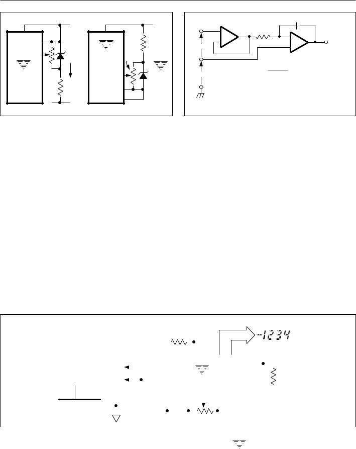
The internal voltage reference potential available at analog common will normally be used to supply the converter's reference. This potential is stable whenever the supply potential is greater than approximately 7V. In applications where an externally-generated reference voltage is desired, refer to Figure 7.
2
3
4
5
6
7
8
TELCOM SEMICONDUCTOR, INC. |
3-193 |
3-1/2 DIGIT A/D CONVERTERS
TC7106
TC7106A
TC7107
TC7107A
V+ |
V+ |
|
V+ |
|
|
|
|
+ |
6.8V |
V+ |
|
VREF |
|
Ω |
|
|
ZENER |
|
6.8k |
– |
|
|
|
|
TC7106A |
|
|
VREF |
|
20kΩ |
|
|
|
TC7107A |
|
|
|
|
|
|
IZ |
+ |
|
TC7106A |
|
VREF |
TC04 |
TC7107A |
|
– |
1.2V |
|
|
||
|
|
VREF |
|
|
|
|
REF |
|
|
COMMON |
|
(a) |
|
(b) |
|
Figure 7. External Reference
|
INPUT |
|
|
|
|
C I |
|
+ |
BUFFER |
RI |
|
|
|
|
|
+ |
|
|
|
– |
|
||
|
– |
|
|
|
|
VI |
|
VIN |
|
|
|
|
+ |
||
|
|
|
|
|
|
||
– |
|
|
|
|
|
INTEGRATOR |
|
|
|
|
|
|
|
|
|
V |
VI = |
|
TI |
[VCM – VIN [ |
|
||
R |
I |
C |
|
||||
CM |
Where: |
|
|
|
I |
4000 |
|
|
|
|
|
|
|
||
|
TI |
= |
INTEGRATION TIME = |
||||
|
|
|
|
|
|
|
fOSC |
|
CI |
= INTEGRATION CAPACITOR |
|||||
|
RI |
= INTEGRATION RESISTOR |
|||||
Figure 9. Common-Mode Voltage Reduces Available Integrator Swing. (VCOM ¹ VIN)
DEVICE PIN FUNCTIONAL DESCRIPTION
Differential Signal Inputs |
full-scale swing. The integrator output will swing within 0.3V |
of V+ or V– without increasing linearity errors. |
|
(V+IN (Pin 31), V–IN (Pin 30)) |
|
The TC7106A/7017A is designed with true differential inputs and accepts input signals within the input stage common mode voltage range (VCM). The typical range is V+ –1.0 to V– +1 V. Common-mode voltages are removed from the system when the TC7106A/TC7107A operates from a battery or floating power source (isolated from measured system) and VIN– is connected to analog common (VCOM): See Figure 8.
In systems where common-mode voltages exist, the 86dB common-mode rejection ratio minimizes error. Com- mon-mode voltages do, however, affect the integrator output level. Integrator output saturation must be prevented. A worst-case condition exists if a large positive VCM exists in conjunction with a full-scale negative differential signal. The negative signal drives the integrator output positive along with VCM (Figure 9). For such applications the integrator output swing can be reduced below the recommended 2.0V
Differential Reference
(VREF+ (Pin 36), VREF– (Pin 35))
The reference voltage can be generated anywhere within the V+ to V– power supply range.
To prevent rollover errors from being induced by large common-mode voltages, CREF should be large compared to stray node capacitance.
The TC7106A/TC7107A circuits have a significantly lower analog common temperature coefficient. This gives a very stable voltage suitable for use as a reference. The temperature coefficient of analog common is 20ppm/°C typically.
SEGMENT |
LCD DISPLAY |
DRIVE |
|
|
|
|
|
|
|
|
|
|
|
|
|
|
|
|
|
|
|
|
|
|
|
|
|
|
|
|
|
|
|
|
|
|
|
|
|
|
|
|
|
|
|
|
|
|
|
|
|
|
|
|
|
|
|
|
|
|
|
|
|
|
|
|
|
|
|
|
|
|
|
|
|
|
|
|
|
|
|
|
|
|
|
|
|
|
|
|
|
|
|
|
|
|
|
|
|
|
|
|
|
|
|
|
|
|
|
|
|
|
|
|
|
|
|
|
|
|
|
|
|
|
|
|
|
|
|
|
|
|
|
|
|
|
|
|
|
|
|
|
|
|
|
|
|
|
|
|
|
|
|
|
|
|
|
|
|
|
|
|
|
|
|
|
|
|
|
|
|
|
|
|
|
|
|
|
|
|
|
|
|
|
|
|
|
|
|
|
|
|
|
|
|
|
|
|
|
|
|
|
|
|
|
|
|
|
|
|
|
|
|
|
|
|
|
|
|
|
|
|
|
|
|
|
|
|
|
|
|
|
|
|
|
|
|
|
|
|
|
|
|
|
|
|
|
|
MEASURED |
|
|
|
|
VBUF |
CAZ |
|
|
VINT |
|
|
|
POL BP |
|
|
|
|
|
|
|
|||||||||||||||||||||
|
|
|
|
|
|
SYSTEM |
|
|
|
V |
+ |
IN |
|
|
|
|
|
|
|
|
|
|
|
|
|
|
|
|
|
|
OSC1 |
|
|
|
|
|
|
|
|||||||||
|
|
|
|
|
|
|
|
|
|
|
|
|
|
|
|
|
|
|
|
|
|
|
|
|
|
|
|
|
|
|
|
|
|
||||||||||||||
|
|
|
|
|
|
V+ |
|
|
|
|
|
|
|
|
|
|
|
|
|
|
|
|
|
|
|
|
|
|
|
|
|
|
|
|
|
|
|
|
|
||||||||
|
|
|
|
|
|
|
|
|
|
|
|
|
|
|
|
|
|
|
|
|
|
|
|
|
|
|
|
|
|
|
|
|
|
|
|
|
|
|
|||||||||
|
|
|
|
|
|
|
|
|
V–IN |
|
TC7106A |
|
|
|
|
|
OSC3 |
|
|
|
|
|
|
|
|
||||||||||||||||||||||
|
|
|
|
|
|
|
|
|
|
|
|
|
|
|
|
|
|
|
|
|
|
|
|||||||||||||||||||||||||
|
|
|
|
|
|
V– |
|
|
|
|
|
|
|
|
|
|
|
|
|
|
|
|
|
||||||||||||||||||||||||
|
|
|
|
|
|
|
GND |
|
|
|
ANALOG |
– |
+ |
|
|
|
|
|
|
|
|
|
OSC2 |
|
|
|
|
|
|
|
|||||||||||||||||
|
|
|
|
|
|
|
|
|
|
|
|
|
|
|
|
|
|
|
|
|
|
|
|
|
|
||||||||||||||||||||||
|
|
+ V |
|
|
|
|
|
|
|
|
COMMON VREF VREF V+ |
|
|
|
|
|
V– |
|
|
|
|
|
|
|
|||||||||||||||||||||||
|
|
|
– |
|
|
|
|
|
|
|
|
|
|
|
|
|
|||||||||||||||||||||||||||||||
|
V |
|
|
|
|
|
|
|
|
|
|
|
|
|
|
|
|
|
|
|
|
|
|
|
|
|
|
|
|
|
|
|
|
|
|
|
|
|
|
|
|
|
|
||||
|
|
|
|
|
|
|
|
|
|
|
|
|
|
|
|
|
|
|
|
|
|
|
|
|
|
|
|
|
|
|
|
|
|
|
|
|
|
|
|
|
|
||||||
|
|
|
|
|
GND |
|
|
|
|
|
|
|
|
|
|
|
|
|
|
|
|
|
|
|
|
|
|
|
|
|
|
|
|
|
|
|
|
|
|
|
|
|
|
|
|
|
|
|
|
POWER |
|
|
|
|
|
|
|
|
|
|
|
|
|
|
|
|
|
|
|
|
|
|
|
|
|
|
|
|
|
|
|
|
|
|
|
|
|
|
|
|
|
||||
|
|
|
|
|
|
|
|
|
|
|
|
|
|
|
|
|
|
|
|
|
|
|
|
|
|
+ |
|
|
|
|
|
|
|
|
|
|
|
|
|
|
|
||||||
|
|
|
|
|
|
|
|
|
|
|
|
|
|
|
|
|
|
|
|
|
|
|
|
|
|
|
|
|
|
|
|
|
|
|
|
|
|
|
|
|
|||||||
|
|
SOURCE |
|
|
|
|
|
|
|
|
|
|
|
|
|
|
|
|
|
|
|
|
|
|
|
|
|
|
9V |
||||||||||||||||||
|
|
|
|
|
|
|
|
|
|
|
|
|
|
|
|
|
|
|
|
|
|
|
|
|
|
|
|
|
|
|
|
|
|
|
|
|
|
|
|
|
|
|
|
|
|
|
|
|
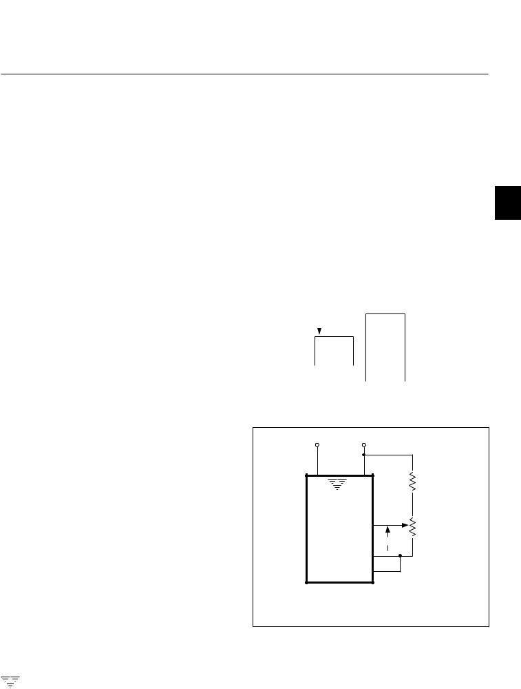
Figure 8. Common-Mode Voltage Removed in Battery Operation with VIN– = Analog Common |
||||||||||||||||||||||||||||||||||||||||||||||
3-194 |
|
|
|
|
|
|
|
|
|
|
|
|
|
|
|
|
|
|
|
|
|
|
|
|
|
|
|
|
|
|
|
|
|
|
|
|
|
TELCOM SEMICONDUCTOR, INC. |
|||||||||
3-1/2 DIGIT A/D CONVERTERS
Analog Common (Pin 32)
The analog common pin is set at a voltage potential approximately 3.0V below V+. The potential is guaranteed to be between 2.7V and 3.35 V below V+. Analog common is tied internally to the N channel FET capable of sinking 20mA. This FET will hold the common line at 3.0V should an external load attempt to pull the common line toward V+. Analog common source current is limited to 10μA. Analog common is therefore easily pulled to a more negative voltage (i.e., below V+ – 3.0V).
The TC7106A connects the internal VIN+ and VIN– inputs to analog common during the auto-zero cycle. During the reference-integrate phase, VIN– is connected to analog common. If VIN– is not externally connected to analog common, a common-mode voltage exists. This is rejected by the converter's 86dB common-mode rejection ratio. In battery operation, analog common and VIN– are usually connected, removing common-mode voltage concerns. In systems where VIN– is connected to the power supply ground or to a given voltage, analog common should be connected to VIN– .
The analog common pin serves to set the analog section reference or common point. The TC7106A is specifically designed to operate from a battery or in any measurement system where input signals are not referenced (float) with respect to the TC7106A power source. The analog common potential of V+ – 3.0V gives a 6 V end of battery life voltage. The common potential has a 0.001%/% voltage coefficient and a 15 Ω output impedance.
With sufficiently high total supply voltage (V+ – V– > 7.0V) analog common is a very stable potential with excellent temperature stability—typically 20ppm/°C. This potential can be used to generate the reference voltage. An external voltage reference will be unnecessary in most cases because of the 50ppm/°C maximum temperature coefficient. See Internal Voltage Reference discussion.
Test (Pin 37)
The TEST pin potential is 5V less than V+. TEST may be used as the negative power supply connection for external CMOS logic. The TEST pin is tied to the internally generated negative logic supply (Internal Logic Ground) through a 500Ω resistor in the TC7106A. The TEST pin load should be no more than 1mA .
If TEST is pulled to V+ all segments plus the minus sign will be activated. Do not operate in this mode for more than several minutes with the TC7106A. With TEST = V+ the LCD segments are impressed with a DC voltage which will destroy the LCD.
The TEST pin will sink about 10mA when pulled to V+.
|
|
|
|
|
|
|
|
|
TC7106 |
1 |
|||
|
|
|
|
|
|
|
|
|
TC7106A |
|
|||
|
|
|
|
|
|
|
|
|
TC7107 |
|
|||
|
|
|
|
|
|
|
|
|
TC7107A |
|
|||
Internal Voltage Reference Stability |
2 |
||||||||||||
The analog common voltage temperature stability has |
|||||||||||||
been significantly improved (Figure 10). The “A” version of |
|||||||||||||
the industry standard circuits allow users to upgrade old |
|
||||||||||||
systems and design new systems without external voltage |
|
||||||||||||
references. External R and C values do not need to be |
|
||||||||||||
changed. Figure 11 shows analog common supplying the |
|
||||||||||||
necessary voltage reference for the TC7106A/TC7107A. |
|
||||||||||||
|
|
|
|
|
|
|
|
|
|
|
|
|
3 |
(ppm/°C) |
200 |
|
|
|
|
|
|
|
|
|
|
|
|
|
|
|
|
|
|
|
|
|
|
|
|||
180 |
|
|
NO |
|
|
|
|
|
|
|
|||
|
|
|
|
|
|
|
|
|
|
||||
|
|
|
|
|
|
|
|
|
|
|
|||
|
160 |
|
|
MAXIMUM |
|
NO MAXIMUM |
|
|
|
||||
|
|
|
SPECIFIED |
|
|
|
|
||||||
|
|
|
|
|
|
|
|||||||
COEFFICIENT |
|
|
|
|
|
|
|
|
SPECIFIED |
|
|
|
|
140 |
|
|
|
|
|
NO MAXIMUM |
|
TYPICAL |
|
|
|
4 |
|
|
|
|
|
|
|
|
|
|
|
|
|
||
|
|
|
|
|
|
|
|
|
|
|
|
|
|
|
120 |
|
|
|
|
|
|
|
|
|
|
|
|
|
|
|
|
|
|
|
|
|
|
|
|
|
|
TEMPERATURE |
100 |
|
|
MAXIMUM |
SPECIFIED |
|
|
|
|
|
|
||
|
|
|
|
|
|
|
|
||||||
80 |
|
|
|
|
|
|
|
|
|||||
|
|
|
LIMIT |
TYPICAL |
|
|
|
|
|
|
|||
|
|
|
|
|
|
|
|
|
|
||||
|
|
|
|
|
|
|
|
|
|
|
|||
|
|
|
|
|
|
|
|
|
|
|
|
|
|
|
60 |
|
|
|
|
|
|
|
|
|
|
|
|
|
|
|
TYPICAL |
|
|
|
|
|
|
|
|||
|
40 |
|
|
|
|
|
|
|
|
|
|||
|
|
|
|
|
|
|
|
|
|
|
|
|
|
|
20 |
|
|
|
|
|
|
|
|
|
|
|
5 |
|
|
|
|
|
TC |
|
ICL7106 |
|
ICL7136 |
|
|
|
|
|
0 |
|
|
|
7106A |
|
|
|
|
|
|||
|
|
|
|
|
|
|
|
|
|
||||
|
|
|
|
|
|
|
|
|
|
|
|
|
|
|
|
|
|
|
|
|
|
|
|
|
|
||
|
Figure 10. Analog Common Temperature Coefficient |
|
|||||||||||
V– |
1 |
|
6 |
V+ |
24kΩ |
||
|
TC7106A |
|
|
|
TC7107A |
|
|
|
+ |
36 |
|
|
VREF |
1kΩ |
|
|
|
VREF |
7 |
|
– |
35 |
|
|
VREF |
|
|
|
ANALOG |
32 |
|
|
COMMON |
|
|
SET VREF = 1/2 VFULL SCALE |
|
||
Figure 11. Internal Voltage Reference Connection
8
TELCOM SEMICONDUCTOR, INC. |
3-195 |
3-1/2 DIGIT A/D CONVERTERS
TC7106
TC7106A
TC7107
TC7107A
POWER SUPPLIES
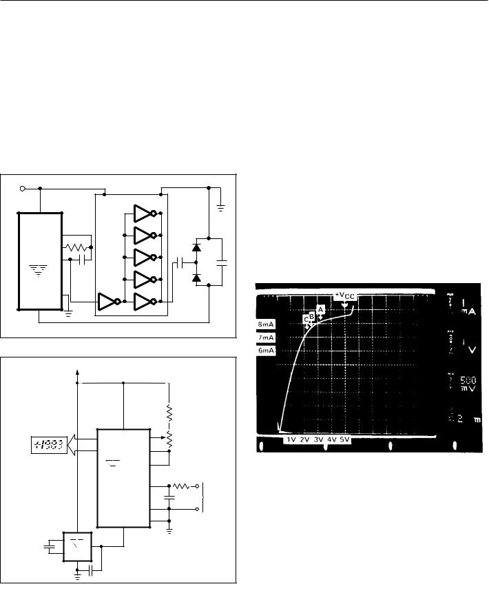
The TC7107A is designed to work from ±5V supplies. However, if a negative supply is not available, it can be generated from the clock output with two diodes, two capacitors, and an inexpensive IC. (Figure 12)
In selected applications a negative supply is not required. The conditions to use a single +5V supply are:
•The input signal can be referenced to the center of the common-mode range of the converter.
•The signal is less than ±1.5V.
•An external reference is used.
The TSC7660 DC to DC converter may be used to
generate – 5 V from +5 V (Figure 13).
V+ |
|
|
|
|
CD4009 |
|
|
V+ |
|
|
|
OSC1 |
|
|
|
OSC2 |
0.047 |
1N914 |
|
OSC3 |
µF |
10 |
+ |
|
|||
|
|
µF |
– |
TC7107A |
|
1N914 |
|
|
|
|
|
GND |
|
|
|
V– |
|
|
|
|
V– = –3.3V |
|
|
Figure 12. Generating Negative Supply From +5 V |
|
||
|
+5 V |
|
|
|
|
|
|
|
1 |
|
|
|
|
|
|
V+ |
+ |
36 |
|
|
|
|
|
|
|
VREF |
|
|
|
|
|
|
|
– |
35 |
|
|
LED |
|
|
|
VREF |
|
|
|
|
|
|
|
32 |
|
|
|
DRIVE |
|
|
COM |
||
|
|
|
|
|
|
|
|
|
|
|
|
TC7107A |
+ |
31 |
|
|
|
|
|
|
|
||
|
|
|
|
|
|
VIN |
|
|
|
|
|
|
|
|
VIN |
|
|
|
|
|
|
– |
30 |
|
|
|
|
|
|
VIN |
|
|
|
|
|
V |
– |
GND |
21 |
|
|
|
|
|
|
|
|
|
2 |
8 |
|
|
26 |
|
|
|
|
|
|
|
|
|
|
10µF |
+ |
|
5 |
(–5 V) |
|
|
|
4 |
TC7660 |
|
|
|
|
|
|
|
|
|
|
|
|
||
|
|
|
|
|
|
|
|
|
|
3 |
|
|
|
*3-1/2 DIGIT ADC |
|
|
|
|
|
|
|
|
|
|
|
+ |
10µF |
|
|
|
|
Figure 13. Negative Power Supply Generation with TC7660
3-196
TC7107 Power Dissipation Reduction
The TC7107A sinks the LED display current and this causes heat to build up in the IC package. If the internal voltage reference is used, the changing chip temperature can cause the display to change reading. By reducing the LED common anode voltage the TC7107A package power dissipation is reduced.
Figure 14 is a photograph of a curve-tracer display showing the relationship between output current and output voltage for a typical TC7107CPL. Since a typical LED has 1.8 volts across it at 7mA, and its common anode is connected to +5V, the TC7107A output is at 3.2V (point A on Figure 13). Maximum power dissipation is 8.1mA x 3.2V x 24 segments = 622mW.
Notice, however, that once the TC7107A output voltage is above two volts, the LED current is essentially constant as output voltage increases. Reducing the output voltage by 0.7V (point B in Figure 14) results in 7.7mA of LED current, only a 5 percent reduction. Maximum power dissipation is only 7.7mA x 2.5 V x 24 = 462mW, a reduction of 26%. An output voltage reduction of 1 volt (point C) reduces LED current by 10% (7.3mA) but power dissipation by 38%! (7.3mA x 2.2V x 24 = 385mW).
Figure 14. TC7107A Output Current vs Output Voltage
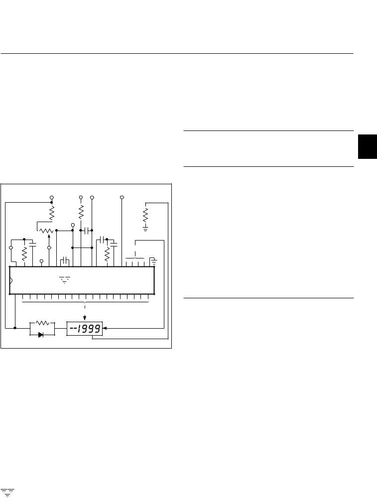
Reduced power dissipation is very easy to obtain. Figure 15 shows two ways: either a 5.1 ohm, 1/4 watt resistor or a 1 Amp diode placed in series with the display (but not in series with the TC7107A). The resistor will reduce the TC7107A output voltage, when all 24 segments are “ON,” to point “C” of Figure 14. When segments turn off, the output voltage will increase. The diode, on the other hand, will result in a relatively steady output voltage, around point “B.”
In addition to limiting maximum power dissipation, the resistor reduces the change in power dissipation as the display changes. This effect is caused by the fact that, as
 TELCOM SEMICONDUCTOR, INC.
3-1/2 DIGIT A/D CONVERTERS
TC7106
TC7106A
TC7107
TC7107A
fewer segments are “ON,” each “ON” output drops more voltage and current. For the best case of six segments (a “111” display) to worst case (a “1888” display) the resistor will change about 230mW, while a circuit without the resistor will change about 470mW. Therefore, the resistor will reduce the effect of display dissipation on reference voltage drift by about 50%.
The change in LED brightness caused by the resistor is almost unnoticeable as more segments turn off. If display brightness remaining steady is very important to the designer, a diode may be used instead of the resistor.
Figure 15. Diode or Resistor Limits Package Power Dissipation
APPLICATIONS INFORMATION
Liquid Crystal Display Sources
Several LCD manufacturers supply standard LCD displays to interface with the TC7106A 3-1/2 digit analog-to- digital converter.
Manufacturer |
Address/Phone |
Part Numbers1 |
Crystaloid |
5282 Hudson Dr. |
C5335, H5535, |
Electronics |
Hudson, OH 44236 |
T5135, SX440 |
|
216/655-2429 |
|
APPLICATIONS INFORMATION
|
+5V |
IN |
|
–5V |
|
|
|
+ |
– |
|
|
|
24kΩ |
1 MΩ |
|
|
150Ω |
|
|
|
|
||
|
1kΩ |
TP3 |
|
|
|
|
|
0.47 |
|
|
|
|
|
|
|
|
|
|
100 |
0.01 |
F |
0.22 |
|
|
|
|
|||
|
pF |
|
F |
|
|
TP5 |
F |
|
|
||
|
|
|
|
||
TP2 |
0.1 |
|
|
DISPLAY |
|
100 |
47 |
|
|||
|
|
|
|
||
kΩ |
TP1 |
F |
Ω |
|
|
|
|
k |
|
|
|
40 |
|
30 |
|
TP |
21 |
|
|
TC7107A |
|
4 |
|
|
|
|
|
|
|
1 |
|
10 |
|
|
20 |
|
|
DISPLAY |
|
|
|
|
5.1Ω 1/4W |
|
|
|
|
|
1N4001 |
|
|
|
|
AND |
720 Palomar Ave. |
FE 0201,0701 |
|
Sunnyvale, CA 94086 |
FE 0203, 2201 |
|
408/523-8200 |
FE 0501 |
|
|
|
Epson |
3415 Kashikawa St. |
LD-B709BZ |
|
Torrance, CA 90505 |
LD-H7992AZ |
|
213/534-0360 |
|
|
|
|
Hamlin, Inc. |
612 E. Lake St. |
3902, 3933, 3903 |
|
Lake Mills, WI 53551 |
|
|
414/648-2361 |
|
|
|
|
Note: 1. Contact LCD manufacturer for full product listing/specifications.
Light Emitting Diode Display Sources
Several LED manufacturers supply seven segment digits with and without decimal point annunciators for the TC7107A.
Manufacturer |
Address |
Display Type |
Hewlett-Packard |
640 Page Mill Rd. |
LED |
Components |
Palo Alto, CA 94304 |
|
|
|
|
AND |
720 Palomar Ave. |
LED |
|
Sunnyvale, CA 94086 |
|
|
|
|
1
2
3
4
5
6
7
8
TELCOM SEMICONDUCTOR, INC. |
3-197 |