Материал: TC7106
3-1/2 DIGIT A/D CONVERTERS
TC7106
TC7106A
TC7107
TC7107A
PIN DESCRIPTION (Cont.)
Pin No. |
Pin No. |
|
|
40-Pin PDIP |
40-Pin PDIP |
|
|
(Normal) |
(Reverse) |
Symbol |
Description |
|
|
|
|
34 |
(7) |
C+REF |
A 0.1μF capacitor is used in most applications. If a large common- |
|
|
|
mode voltage exists (for example, the V–IN pin is not at analog |
|
|
|
common), and a 200mV scale is used, a 1μF capacitor is recom- |
|
|
|
mended and will hold the roll-over error to 0.5 count. |
|
|
|
|
35 |
(6) |
VREF– |
See pin 36. |
36 |
(5) |
V+ |
The analog input required to generate a full-scale output (1999 |
|
|
REF |
counts). Place 100mV between pins 35 and 36 for 199.9mV |
|
|
|
|
|
|
|
full-scale. Place 1V between pins 35 and 36 for 2V full scale. See |
|
|
|
paragraph on REFERENCE VOLTAGE. |
|
|
|
|
37 |
(4) |
Test |
Lamp test. When pulled HIGH (to V+) all segments will be turned on |
|
|
|
and the display should read –1888. It may also be used as a negative |
|
|
|
supply for externally-generated decimal points. See paragraph under |
|
|
|
TEST for additional information. |
|
|
|
|
38 |
(3) |
OSC3 |
See pin 40. |
39 |
(2) |
OSC2 |
See pin 40. |
40 |
(1) |
OSC1 |
Pins 40, 39, 38 make up the oscillator section. For a 48kHz clock |
(3 readings per section), connect pin 40 to the junction of a 100kΩ resistor and a 100pF capacitor. The 100kΩ resistor is tied to pin 39 and the 100pF capacitor is tied to pin 38.
GENERAL THEORY OF OPERATION DUAL SLOPE CONVERSION PRINCIPLES
(All Pin Designations Refer to the 40-Pin DIP)
The TC7106A and TC7107A are dual slope, integrating analog-to-digital converters. An understanding of the dual slope conversion technique will aid in following the detailed operation theory.
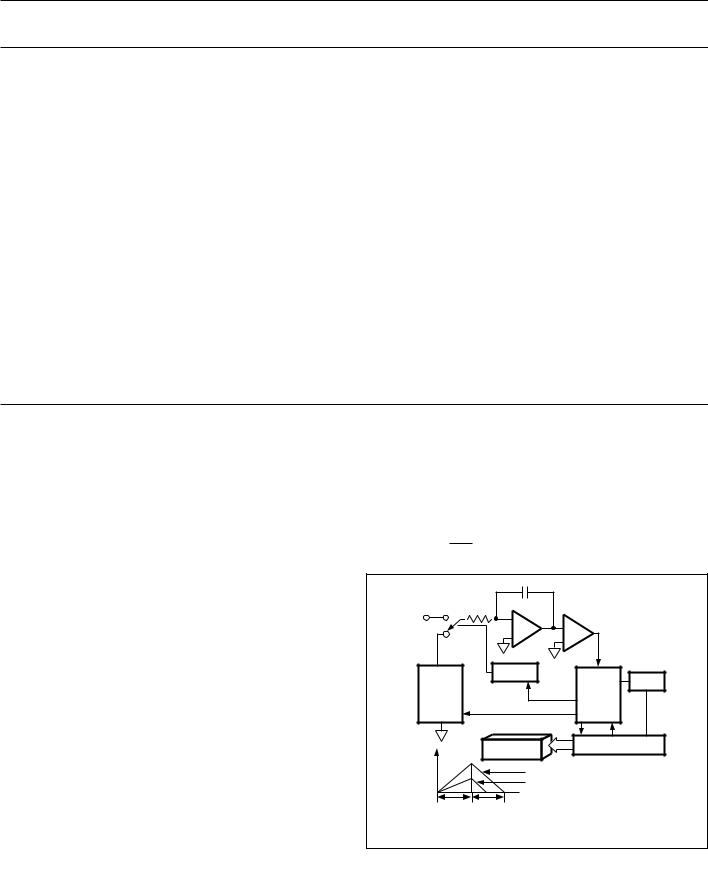
The conventional dual slope converter measurement cycle has two distinct phases:
•Input Signal Integration
•Reference Voltage Integration (Deintegration)
The input signal being converted is integrated for a fixed time period (TSI). Time is measured by counting clock pulses. An opposite polarity constant reference voltage is then integrated until the integrator output voltage returns to zero. The reference integration time is directly proportional to the input signal (TRI). (Figure 2A).
In a simple dual slope converter a complete conversion requires the integrator output to “ramp-up” and “rampdown.”
A simple mathematical equation relates the input signal, reference voltage and integration time:
|
TSI |
|
1 |
ò 0 VIN(t)dt = |
VRTRI |
RC |
RC |
3-188
where:
VR = Reference Voltage
TSI = Signal Integration Time (Fixed)
TRI = Reference Voltage Integration Time (Variable)
For a constant VIN:
TRI
TSI
ANALOG |
C |
|
|
|
|
||
INPUT |
INTEGRATOR |
|
|
SIGNAL |
COMPARATOR |
||
|
|||
|
– |
||
|
– |
||
|
|
|
+ |
+ |
|
|
|
|
|
+/– |
SWITCH |
|
|
|
|
|
|
|
DRIVER |
|
CLOCK |
REF |
|
PHASE |
|
|
CONTROL |
||
VOLTAGE |
|
CONTROL |
LOGIC |
|
POLARITY CONTROL |
|
|
INTEGRATOR OUTPUT |
DISPLAY |
COUNTER |
|
||
VIN |
≈ VFULL SCALE |
|
VIN |
≈ 1/2 VFULL SCALE |
|
|
|
FIXED VARIABLE
SIGNAL REFERENCE
INTEGRATE INTEGRATE
TIME TIME
Figure 2A. Basic Dual Slope Converter
 TELCOM SEMICONDUCTOR, INC.
3-1/2 DIGIT A/D CONVERTERS
TC7106 1 TC7106A
TC7107
TC7107A
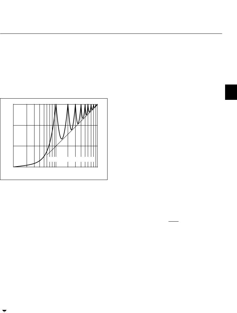
The dual slope converter accuracy is unrelated to the integrating resistor and capacitor values as long as they are stable during a measurement cycle. An inherent benefit is noise immunity. Noise spikes are integrated or averaged to zero during the integration periods. Integrating ADCs are immune to the large conversion errors that plague successive approximation converters in high-noise environments. Interfering signals with frequency components at multiples of the averaging period will be attenuated. Integrating ADCs commonly operate with the signal integration period set to a multiple of the 50/60 Hz power line period. (Figure 2B)
|
30 |
|
|
(dB) |
|
|
|
MODE REJECTION |
20 |
|
|
10 |
|
|
|
NORMAL |
|
|
|
|
T = MEASUREMENT PERIOD |
||
|
|
|
|
|
0 |
|
|
|
0.1/T |
1/T |
10/T |
|
|
INPUT FREQUENCY |
|
Figure 2B. Normal-Mode Rejection of Dual Slope Converter
ANALOG SECTION
In addition to the basic signal integrate and deintegrate cycles discussed, the circuit incorporates an auto-zero cycle. This cycle removes buffer amplifier, integrator, and comparator offset voltage error terms from the conversion. A true digital zero reading results without adjusting external potentiometers. A complete conversion consists of three cycles: an auto-zero, signal-integrate and reference-inte- grate cycle.
Auto-Zero Cycle
During the auto-zero cycle the differential input signal is disconnected from the circuit by opening internal analog gates. The internal nodes are shorted to analog common (ground) to establish a zero-input condition. Additional analog gates close a feedback loop around the integrator and comparator. This loop permits comparator offset voltage error compensation. The voltage level established on CAZ compensates for device offset voltages. The offset error referred to the input is less than 10μV.
The auto-zero cycle length is 1000 to 3000 counts.
 TELCOM SEMICONDUCTOR, INC.
Signal Integrate Cycle
When the auto-zero loop is opened, the internal differential inputs connect to VIN+ and VIN– . The differential input signal is integrated for a fixed time period. The signal integration period is 1000 counts. The externally set clock frequency is divided by four before clocking the internal counters. The integration time period is:
TSI = |
4 |
x 1000 |
|
fOSC |
|||
|
|
where:
fOSC = External Clock Frequency
The differential input voltage must be within the device common-mode range (1V of either supply) when the converter and measured system share the same power supply common (ground). If the converter and measured system do not share the same power supply common, VIN– should be tied to analog common.
Polarity is determined at the end of the signal integrate phase. The sign bit is a true polarity indication in that signals less than 1 LSB are correctly determined. This allows precision null detection, limited only by device noise and auto-zero residual offsets.
Reference Integrate Cycle
The final phase is reference integrate or de-integrate. VIN– is internally connected to analog common and VIN+ is connected across the previously charged reference capacitor. Circuitry within the chip ensures that the capacitor will be connected with the correct polarity to cause the integrator output to return to zero. The time required for the output to return to zero is proportional to the input signal and is between 0 and 2000 counts. The digital reading displayed is:
VIN
1000 x VREF
DIGITAL SECTION (TC7106A)
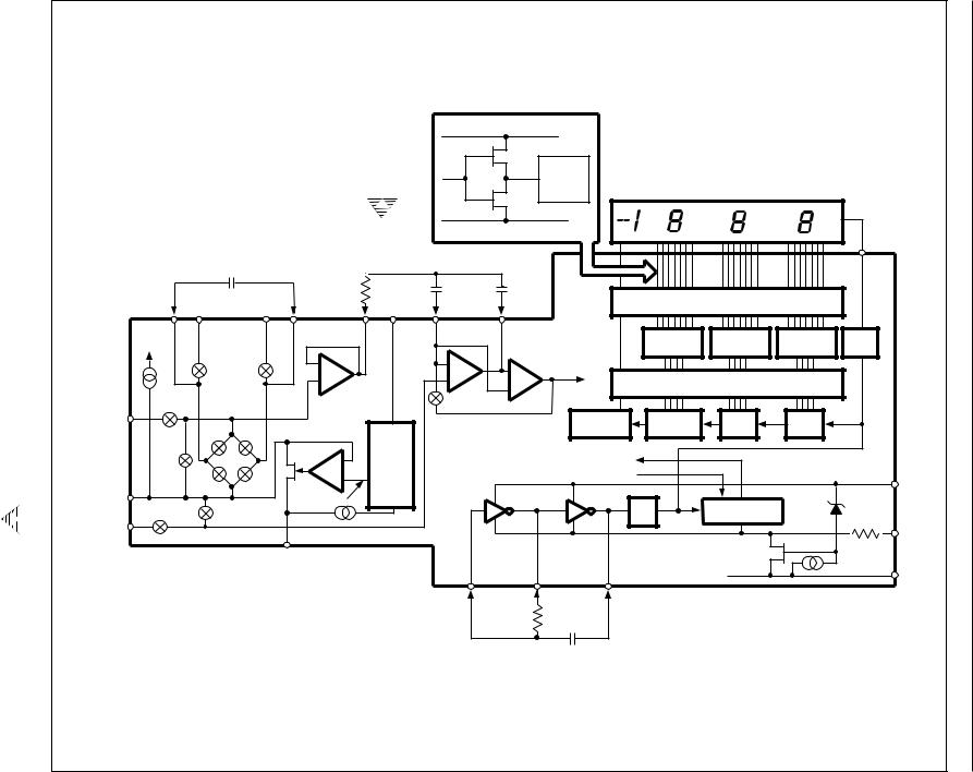
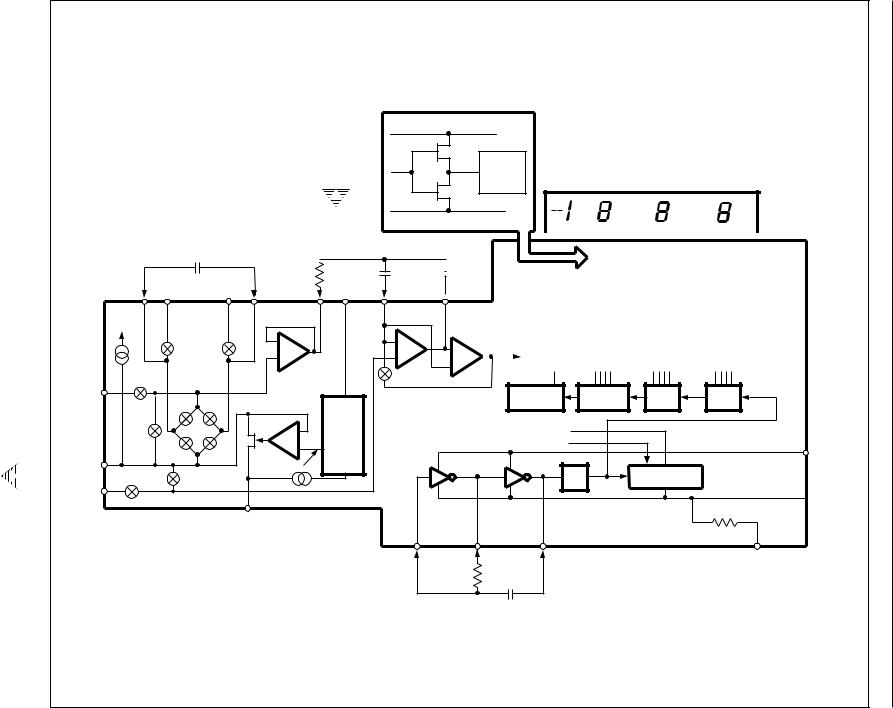
The TC7106A (Figure 3) contains all the segment drivers necessary to directly drive a 3 -1/2 digit liquid crystal display (LCD). An LCD backplane driver is included. The backplane frequency is the external clock frequency divided by 800. For three conversions/second the backplane frequency is 60Hz with a 5V nominal amplitude. When a segment driver is in phase with the backplane signal the segment is “OFF.” An out of phase segment drive signal causes the segment to be “ON” or visible. This AC drive configuration results in negligible DC voltage across each LCD segment. This insures long LCD display life. The polarity segment driver is “ON” for negative analog inputs. If VIN+ and VIN– are reversed, this indicator will reverse.
3-189
2
3
4
5
6
7
8
190-3
Diagram Block TC7106A .3 Figure
.INC SEMICONDUCTOR, TELCOM
TYPICAL SEGMENT OUTPUT
V+
|
|
|
|
|
|
|
|
0.5mA |
|
|
|
|
|
|
|
|
SEGMENT |
|
|
|
|
|
|
|
|
OUTPUT |
|
|
|
|
|
|
|
|
LCD DISPLAY |
|
|
|
|
|
|
|
|
2mA |
|
|
|
|
TC7106A |
INTERNAL DIGITAL GROUND |
|||
|
|
|
|
|
|
|
|
BACKPLANE |
|
|
|
|
|
|
|
|
21 |
+ |
+ |
CREF |
– |
|
RINT |
+ |
CAZ |
CINT |
– |
VBUFF |
|
|
LCD SEGMENT DRIVERS |
||||
C REF |
VREF |
VREF |
CREF |
V |
|
|
VINT |
|
|
34 |
36 |
35 |
33 |
28 |
1 |
29 |
27 |
|
|
|
|
|
|
|
|
|
|
|
|
|
INTEGRATOR |
TO |
7 SEGMENT |
7 SEGMENT |
7 SEGMENT |
200 |
|
|
|
|
|
|
|
|
|
|
|
DECODE |
DECODE |
DECODE |
|
|
|
|
|
|
|
– |
|
|
– |
|
DIGITAL |
|
|
|
|
|
|
10 |
A/Z |
A/Z |
|
|
+ |
SECTION |
|
|
|
|
|
||
|
+ |
|
|
+ |
|
|
|
|
|
|||||
|
|
|
|
|
|
|
|
|
DATA LATCH |
|
|
|
||
|
A |
|
|
|
|
|
– |
|
|
|
|
|
||
|
|
|
|
|
|
|
A/Z |
|
|
|
|
|
|
|
|
|
|
|
|
|
|
|
|
|
|
|
|
|
|
+ |
31 |
|
|
|
|
|
COMPARATOR |
|
|
|
|
|
|
|
|
|
|
|
|
|
|
|
|
|
|
|
|||
V IN |
|
DE |
DE |
|
|
|
THOUSANDS |
HUNDREDS |
TENS |
UNITS |
|
|
||
|
INT |
(–) |
(+) |
|
|
|
|
|
|
|
|
|
|
|
|
A/Z |
|
|
– |
LOW |
|
|
|
TO SWITCH DRIVERS |
|
|
|
|
|
|
|
|
TEMPCO |
|
|
|
|
|
|
|
||||
|
|
|
|
+ |
VREF |
|
|
FROM COMPARATOR OUTPUT |
|
|
|
1 |
V+ |
|
ANALOG |
32 |
DE (+) |
DE (–) |
|
|
|
CLOCK |
|
|
|
|
|||
V+– 3.0V |
|
|
|
|
|
|
|
|
|
|||||
|
|
|
|
|
|
fOSC |
|
|
|
|
|
|||
COMMON |
|
|
|
|
|
|
|
4 |
CONTROL LOGIC |
|
6.2V |
|
||
– |
30 |
AZ & DE (±) |
|
|
|
|
|
|
|
|
||||
|
|
|
|
|
|
|
|
|
37 |
|
||||
V IN |
|
|
|
26 |
|
|
|
|
|
|
|
|
TEST |
|
|
INT |
|
|
|
|
|
|
INTERNAL DIGITAL GOUND |
|
500Ω |
||||
|
|
|
V – |
|
|
|
|
|
|
|||||
|
|
|
|
|
|
|
|
|
|
VTH |
|
|
|
|
|
|
|
|
|
|
|
|
|
|
|
= 1V |
|
26 |
|
|
|
|
|
|
|
|
|
|
|
|
|
|
V– |
|
|
|
|
|
|
|
|
40 |
39 |
38 |
|
|
|
|
|
|
|
|
|
|
|
|
|
|
|
|
|
|||
|
|
|
|
|
|
|
OSC1 |
OSC2 |
OSC3 |
|
|
|
|
|
|
|
|
|
|
|
|
|
ROSC |
COSC |
|
|
|
|
|
|
|
|
|
|
|
|
|
|
|
|
|
|
|
|
TC7107A |
TC7107 |
TC7106A |
TC7106 |
CONVERTERS A/D DIGIT 1/2-3
3-1/2 DIGIT A/D CONVERTERS
TC7106 1 TC7106A
TC7107
TC7107A
When the TEST pin on the TC7106A is pulled to V+, all segments are turned “ON.” The display reads –1888. During this mode the LCD segments have a constant DC voltage impressed. DO NOT LEAVE THE DISPLAY IN THIS MODE FOR MORE THAN SEVERAL MINUTES! LCD displays may be destroyed if operated with DC levels for extended periods.
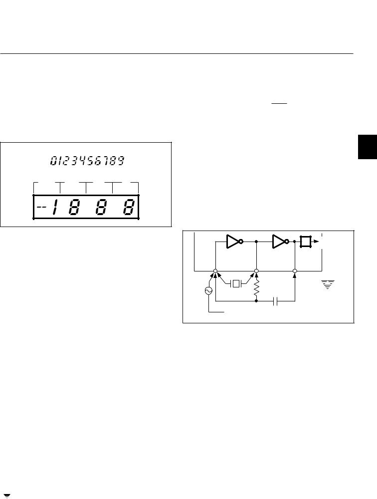
The display font and the segment drive assignment are shown in Figure 4.
DISPLAY FONT
1000's |
100's |
10's |
1's |
Figure 4. Display Font and Segment Assignment
In the TC7106A, an internal digital ground is generated from a 6 volt zener diode and a large P channel source follower. This supply is made stiff to absorb the large capacitive currents when the backplane voltage is switched.
DIGITAL SECTION (TC7107A)
Figure 5 shows the TC7107A. It is designed to drive common anode LEDs. It is identical to the TC7106A except that the regulated supply and backplane drive have been eliminated and the segment drive is typically 8mA. The 1000's output (pin 19) sinks current from two LED segments, and has a 16mA drive capability.
In both devices, the polarity indication is “ON” for negative analog inputs. If VIN– and VIN+ are reversed, this indication can be reversed also, if desired.
The display font is the same as the TC7106A.
System Timing
The oscillator frequency is divided by 4 prior to clocking the internal decade counters. The three-phase measurement cycle takes a total of 4000 counts or 16000 clock pulses. The 4000 count cycle is independent of input signal magnitude.
Each phase of the measurement cycle has the following length:
•Auto-Zero Phase: 1000 to 3000 Counts
(4000 to 12000 Clock Pulses)
For signals less than full-scale, the auto-zero phase is assigned the unused reference integrate time period.
 TELCOM SEMICONDUCTOR, INC.
•Signal Integrate: 1000 Counts
(4000 Clock Pulses) |
2 |
|
|
This time period is fixed. The integration period is: |
|
TSI = 4000 [ fOSC1 ]
Where fOSC is the externally set clock frequency.
•Reference Integrate: 0 to 2000 Counts
|
(0 to 8000 Clock Pulses) |
3 |
The TC7106A/7107A are drop-in replacements for the |
||
7106/7107 parts. External component value changes are |
|
|
not required to benefit from the low drift internal reference. |
|
|
Clock Circuit |
|
|
Three clocking methods may be used: |
4 |
|
1. |
An external oscillator connected to pin 40. |
|
2. |
A crystal between pins 39 and 40. |
|
3. |
An R-C oscillator using all three pins. |
|
|
|
|
÷ 4 |
TO |
|
|
|
|
COUNTER |
|
40 |
39 |
38 |
5 |
|
CRYSTAL |
|
|
|
|
|
|
|
|
EXT |
|
|
|
TC7106A |
OSC |
RC NETWORK |
|
|
|
|
|
|
|
TC7107A |
 TO TEST PIN ON TSC7106A
TO GND PIN ON TSC7107A
Figure 6. Clock Circuits
COMPONENT VALUE SELECTION |
6 |
|
|
Auto-Zero Capacitor –CAZ |
|
The CAZ capacitor size has some influence on system |
|
noise. A 0.47mF capacitor is recommended for 200mV full- |
|
scale applications where 1 LSB is 100mV. A 0.047mF capaci- |
|
tor is adequate for 2.0V full-scale applications. A mylar |
|
dielectric capacitor is adequate. |
7 |
Reference Voltage Capacitor –CREF |
The reference voltage used to ramp the integrator output voltage back to zero during the reference-integrate cycle is stored on CREF. A 0.1mF capacitor is acceptable when VIN– is tied to analog common. If a large common-mode voltage exists (VREF– ¹ analog common) and the application
requires 200mV full-scale, increase CREF to 1.0 mF. Rollover 8 error will be held to less than 1/2 count. A mylar dielectric capacitor is adequate.
3-191
192-3
|
|
|
|
|
|
|
TC7107A |
|||
Figure |
|
|
|
CREF |
|
|
RINT |
|
|
|
|
+ |
|
+ |
– |
– |
VBUFF |
|
+ |
|
|
|
C REF |
VREF |
VREF |
CREF |
V |
|
|
|||
.5 |
|
|
34 |
36 |
35 |
33 |
|
28 |
|
1 |
|
|
|
|
|
||||||
TC7107A |
|
10 |
|
A/Z |
A/Z |
– |
|
|
|
|
|
|
+ |
|
|
|
|
||||
|
A |
|
|
|
|
|
|
|
||
Block |
V + |
31 |
|
|
|
|
|
|
|
|
|
|
DE |
DE |
|
|
|
|
|
||
Diagram |
IN |
|
|
|
|
|
|
|
||
|
INT |
|
(–) |
(+) |
|
|
|
|
|
|
|
A/Z |
|
|
|
|
– |
LOW |
|
|
|
|
|
|
|
|
TEMPCO |
|||||
|
|
|
|
|
|
+ |
VREF |
|
||
|
|
|
|
|
|
|
|
|||
|
|
32 |
|
DE (+) |
DE (–) |
|
|
|
|
|
|
ANALOG |
|
V+– 3.0V |
|
|
|
||||
|
|
|
|
|
|
|
|
|||
|
COMMON |
|
|
|
|
|
|
|
||
|
|
|
|
|
|
|
|
|
|
|
|
– |
30 |
|
AZ & DE (±) |
|
|
|
|
|
|
TELCOM |
V IN |
|
|
|
|
26 |
|
|
|
|
|
INT |
|
|
|
|
|
|
|
||
|
|
|
|
|
V – |
|
|
|
|
|
|
|
|
|
|
|
|
|
|
|
|
.INC SEMICONDUCTOR,
TYPICAL SEGMENT OUTPUT
V+
0.5mA
SEGMENT
OUTPUT
LED DISPLAY
8mA
INTERNAL DIGITAL GROUND
|
CAZ |
|
|
|
|
CINT |
|
|
|
|
|
||
|
|
|
|
|
 VINT
VINT
29 |
27 |
|
|
||
INTEGRATOR |
||
– |
+ |
|
+ |
||
– |
||
A/Z |
||
|
||
|
COMPARATOR |
|
|
|
|
|
|
|
|
|
|
|
|
|
|
|
|
|
|
|
|
|
|
|
|
|
|
|
|
|
|
|
|
|
|
|
|
|
|
|
|
|
|
|
|
|
|
LCD SEGMENT DRIVERS |
|
|||||||||||||||||||||
|
|
|
|
|
|
|
|
|
|
|
|
|
|
|
|
|
|
|
|
|
|
|
|
|
|
|
|
|
|
|
|
|
|
|
|
|
|
|
|
|
|
|
|
|
|
|
|
|
|
|
|
|
|
|
|
|
|
|
|
|
|
|
|
|
|
|
|
|
|
|
|
|
|
|
7 SEGMENT |
|
7 SEGMENT |
|
7 SEGMENT |
|
|||||||||||||||||||||
|
TO |
|
|
DECODE |
|
DECODE |
|
|
DECODE |
|
|||||||||||||||||||||||
|
DIGITAL |
|
|
|
|
|
|
|
|
|
|
|
|
|
|
|
|
|
|
|
|
|
|
|
|
|
|
|
|
|
|||
SECTION |
|
|
|
|
|
|
|
|
|
|
|
|
|
|
|
|
|
|
|
|
|
|
|
|
|
|
|
|
|
|
|||
|
|
|
|
|
|
|
|
|
|
|
|
|
|
|
DATA LATCH |
|
|
|
|
|
|
|
|
|
|||||||||
|
|
|
|
|
|
|
|
|
|
|
|
|
|
|
|
|
|
|
|
|
|
|
|
||||||||||
|
|
|
|
|
|
|
|
|
|
|
|
|
|
|
|
|
|
|
|
|
|
|
|
|
|
|
|
|
|
|
|
|
|
THOUSANDS |
HUNDREDS |
TENS |
UNITS |
TO SWITCH DRIVERS 
FROM COMPARATOR OUTPUT 1 V+ CLOCK
fOSC |
4 |
LOGIC CONTROL |
|
||
|
|
21 |
|
|
DIGITAL GOUND |
DIGITAL |
|
|
GROUND |
|
|
|
500Ω |
|
40 |
39 |
38 |
37 |
OSC1 |
OSC2 |
OSC3 |
TEST |
|
ROSC |
COSC |
|
|
|
|
TC7107A |
TC7107 |
TC7106A |
TC7106 |
CONVERTERS A/D DIGIT 1/2-3