Материал: opt202
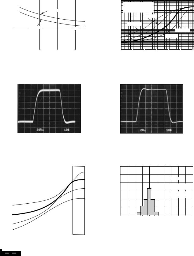
TYPICAL PERFORMANCE CURVES
At TA = +25°C, VS = ±15V, λ = 650nm, unless otherwise noted.
QUIESCENT CURRENT vs TEMPERATURE
|
0.6 |
|
|
|
|
|
|
|
|
|
|
|
|
|
|
|
|
|
|
|
|
|
|
|
|
|
|
|
|
|
|
|
0.5 |
|
|
|
|
|
|
|
|
|
|
|
|
|
|
|
|
|
|
|
|
|
|
|
|
|
|
|
|
|
|
(mA) |
|
|
|
|
|
|
|
VS = ±15V |
|
|
|
|
|
||
|
|
|
|
|
|
|
|
|
|
|
|
|
|||
0.4 |
|
|
|
|
|
|
|
|
|
|
|
|
|
|
|
Current |
|
|
|
|
|
|
|
|
|
|
|
|
|
|
|
0.3 |
|
|
|
|
|
|
|
|
|
|
|
|
|
|
|
|
|
|
|
|
|
|
|
|
|
|
|
|
|
||
|
|
|
V |
S = ±2.25V |
|
|
|
|
|
|
|
|
|||
Quiescent |
|
|
|
|
|
|
|
|
|
Dice |
|
|
|||
0.2 |
|
|
|
|
|
|
|
|
|
|
|
||||
|
|
|
|
|
|
|
|
|
|
|
|
||||
|
|
|
|
|
|
|
|
|
|
|
|
|
|
||
|
|
|
|
|
|
|
|
|
|
|
|
|
|
|
|
|
0.1 |
|
|
|
|
|
|
|
|
|
|
|
|
|
|
|
|
|
|
|
|
|
|
|
|
|
|
|
|
|
|
|
|
|
|
|
|
|
|
|
|
|
|
|
|
|
|
|
0 |
|
|
|
|
|
|
|
|
|
|
|
|
|
|
|
|
|
|
|
|
|
|
|
|
|
|
|
|
|
|
|
|
–50 |
–25 |
0 |
25 |
50 |
75 |
100 |
125 |
||||||
|
–75 |
||||||||||||||
|
|
|
|
|
|
|
Temperature (°C) |
|
|
|
|
|
|||
(CONT)
|
|
|
OUTPUT NOISE VOLTAGE |
|
|
||
|
|
|
vs MEASUREMENT BANDWIDTH |
|
|
||
|
10–2 |
|
|
|
|
|
|
|
|
Dotted lines indicate |
|
|
|
|
|
|
10–3 |
noise measured beyond |
|
|
|
|
|
(Vrms) |
the signal bandwidth. |
|
|
|
|
||
10–4 |
|
RF = 10MΩ |
|
|
|
||
Voltage |
10–5 |
RF = 100MΩ |
|
|
|
|
|
Noise |
|
|
|
|
RF = 100kΩ |
|
|
10–6 |
|
|
|
RF = 1MΩ |
|
|
|
|
|
|
|
|
|
|
|
|
10–7 |
|
|
|
|
|
|
|
1 |
10 |
100 |
1k |
10k |
100k |
1M |
|
|
|
Frequency (Hz) |
|
|
||
SMALL-SIGNAL RESPONSE |
LARGE-SIGNAL RESPONSE |
20mV/div
10μs/div
|
|
|
|
|
|
|
|
|
|
NOISE EFFECTIVE POWER |
|
|
|
|
|
|
|
|
||||||||||||||||
|
|
|
|
|
|
|
|
|
vs MEASUREMENT BANDWIDTH |
|
|
|
|
|
|
|
|
|||||||||||||||||
|
10–7 |
|
|
|
|
|
|
|
|
|
|
|
|
|
|
|
|
|
|
|
|
|
|
|
|
|
|
|
|
|
|
|
|
|
|
|
|
|
Dotted lines indicate |
|
|
|
|
|
|
|
|
|
|
|
|
|
|
|
|
|
|
RF = 100kΩ |
|||||||||||
|
|
|
|
|
|
|
|
|
|
|
|
|
|
|
|
|
|
|
|
|
||||||||||||||
|
10–8 |
|
noise measured beyond |
|
|
|
|
|
|
|
|
|
|
|
|
|
|
|
|
|
|
|||||||||||||
|
|
|
|
|
|
|
|
|
|
|
|
|
|
|
|
|
|
|
|
|||||||||||||||
|
|
|
the signal bandwidth. |
|
|
|
|
|
|
|
|
|
|
|
|
|
|
|
|
|
|
RF = 1MΩ |
||||||||||||
|
|
|
|
|
|
|
|
|
|
|
|
|
|
|
|
|
|
|
|
|||||||||||||||
|
|
|
|
|
|
|
|
|
|
|
|
|
|
|
|
|
|
|
|
|||||||||||||||
(W) |
10–9 |
|
|
|
|
λ |
= 650nm |
|
|
|
|
|
|
|
|
|
|
|
|
|
|
|
|
|
|
|||||||||
|
|
|
|
|
|
|
|
|
|
|
|
|
|
|
|
|
|
|
||||||||||||||||
|
|
|
|
|
|
|
|
|
|
|
|
|
|
|
|
|
|
|
|
|
|
|
|
|
|
|
|
|
|
|
|
RF = 10MΩ |
||
|
|
|
|
|
|
|
|
|
|
|
|
|
|
|
|
|
|
|
|
|
|
|
|
|
|
|
|
|
|
|
|
|||
Power |
|
|
|
|
|
|
|
|
|
|
|
|
|
|
|
|
|
|
|
|
|
|
|
|
|
|
|
|
|
|
|
|
||
|
|
|
|
|
|
|
|
|
|
|
|
|
|
|
|
|
|
|
|
|
|
|
|
|
|
|
|
|
|
|
|
|||
10–10 |
|
|
|
|
|
|
|
|
|
|
|
|
|
|
|
|
|
|
|
|
|
|
|
|
|
|
|
|
|
|
|
|
||
|
|
|
|
|
|
|
|
|
|
|
|
|
|
|
|
|
|
|
|
|
|
|
|
|
|
|
|
|
|
|
|
|||
|
|
|
|
|
|
|
|
|
|
|
|
|
|
|
|
|
|
|
|
|
|
|
|
|
|
|
|
|
|
|
|
RF = 100MΩ |
||
|
|
|
|
|
|
|
|
|
|
|
|
|
|
|
|
|
|
|
|
|
|
|
|
|
|
|
|
|
|
|
|
|||
|
|
|
|
|
|
|
|
|
|
|
|
|
|
|
|
|
|
|
|
|
|
|
|
|
|
|
|
|
|
|
|
|||
|
|
|
|
|
|
|
|
|
|
|
|
|
|
|
|
|
|
|
|
|
|
|
|
|
|
|
|
|
|
|
|
|||
EffectiveNoise |
10–12 |
|
|
|
|
|
|
|
|
|
|
|
|
|
|
|
|
|
|
|
|
|
|
|
|
|
|
|
|
|
|
|
|
|
|
|
|
|
|
|
|
|
|
|
|
|
|
|
|
|
|
|
|
|
|
|
|
|
|
|
|
|
|
|
|
|
|||
|
|
|
|
|
|
|
|
|
|
|
|
|
|
|
|
|
|
|
|
|
|
|
|
|
|
|
|
|
|
|
|
|
||
|
|
|
|
|
|
|
|
|
|
|
|
|
|
|
|
|
|
|
|
|
|
|
|
|
|
|
|
|
|
|
|
|
||
|
10–11 |
|
|
|
|
|
|
|
|
|
|
|
|
|
|
|
|
|
|
|
|
|
|
|
|
|
|
|
|
|
|
|
|
|
|
|
|
|
|
|
|
|
|
|
|
|
|
|
|
|
|
|
|
|
|
|
|
|
|
|
|
|
|
|
|
|
|
|
|
|
|
|
|
|
|
|
|
|
|
|
|
|
|
|
|
|
|
|
|
|
|
|
|
|
|
|
|
|
|
|
|
|
|
|
|
10–13 |
|
|
|
|
|
|
|
|
|
|
|
|
|
|
|
|
|
|
|
|
|
|
|
|
|
|
|
|
|
|
|
|
|
|
|
|
|
|
|
|
|
|
|
|
|
|
|
|
|
|
|
|
|
|
|
|
|
|
|
|
|
|
|
|
|
|
|
|
|
|
|
|
|
|
|
|
|
|
|
|
|
|
|
|
|
|
|
|
|
|
|
|
|
|
|
|
|
|
|
|
|
|
|
|
|
|
|
|
|
|
|
|
|
|
|
|
|
|
|
|
|
|
|
|
|
|
|
|
|
|
|
|
|
|
|
|
|
|
|
|
|
|
|
|
|
|
|
|
|
|
|
|
|
|
|
|
|
|
|
|
|
|
|
|
|
|
|
|
|
|
|
|
|
|
|
|
|
|
|
|
|
|
|
|
|
|
|
|
|
|
|
|
|
|
|
|
|
|
|
|
|
|
|
|
|
|
|
|
|
|
|
|
|
|
|
|
|
|
|
|
|
|
|
|
|
|
|
|
|
|
|
|
|
|
|
|
|
|
|
|
|
|
|
|
|
|
|
|
|
|
|
|
|
|
|
|
|
|
|
|
|
|
|
|
|
|
|
|
|
|
|
|
|
|
|
|
|
|
|
|
|
|
|
|
|
|
|
|
|
|
|
|
|
|
|
|
|
|
|
|
|
|
|
|
|
|
|
|
|
|
|
|
|
|
|
|
|
|
|
|
|
|
|
|
|
|
|
|
|
|
|
|
|
|
|
|
|
|
|
|
|
|
|
|
|
|
|
|
|
10–14 |
|
|
|
|
|
|
|
|
|
|
|
|
|
|
|
|
|
|
|
|
|
|
|
|
|
|
|
|
|
|
|
|
|
|
|
|
|
|
|
|
|
|
|
|
|
|
|
|
|
|
|
|
|
|
|
|
|
|
|
|
|
|
|
|
|
|
|
|
|
|
|
|
|
|
|
|
|
|
|
|
|
|
|
|
|
|
|
|
|
|
|
|
|
|
|
|
|
|
|
|
|
|
|
|
|
|
|
|
|
|
|
|
|
|
|
|
|
|
|
|
|
|
|
|
|
|
|
|
|
|
|
|
|
|
|
|
|
|
|
1 |
10 |
100 |
|
|
1k |
10k |
100k |
1M |
|||||||||||||||||||||||||
Frequency (Hz)


 ®
®
Units (%)
2V/div
10μs/div
DISTRIBUTION OF RESPONSIVITY
60
50
λ = 650nm
40
Distribution Totals
100%
30
Laboratory Test
Data
20
10
0
0.43 |
0.44 |
0.45 |
0.46 |
0.47 |
0.48 |
Responsivity (A/W)
|
OPT202 |
6 |
|
APPLICATIONS INFORMATION
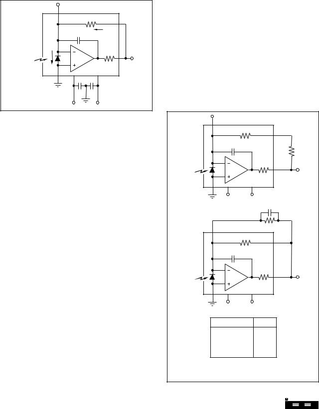
Figure 1 shows the basic connections required to operate the OPT202. Applications with high-impedance power supplies may require decoupling capacitors located close to the device pins as shown. Output is zero volts with no light and increases with increasing illumination.
(Pin available on DIP only)
|
|
1MΩ |
RF |
ID is proportional |
(0V) |
3pF |
ID |
|
|||
|
|
|
|
to light intensity |
|
|
|
(radiant power). |
|
|
175Ω |
λ |
ID |
|
|
|
VO |
||
|
|
||
|
|
VO = ID RF |
|
|
|
|
|
|
|
|
OPT202 |
|
|
0.1µF 0.1µF |
|
+15V –15V
FIGURE 1. Basic Circuit Connections.
Photodiode current, ID, is proportional to the radiant power or flux (in watts) falling on the photodiode. At a wavelength of 650nm (visible red) the photodiode Responsivity, RI, is approximately 0.45A/W. Responsivity at other wavelengths is shown in the typical performance curve “Responsivity vs Wavelength.”
The typical performance curve “Output Voltage vs Radiant Power” shows the response throughout a wide range of radiant power. The response curve “Output Voltage vs Irradiance” is based on the photodiode area of 5.23 x 10–m6 2.
The OPT202’s voltage output is the product of the photodiode current times the feedback resistor, (IDRF). The internal feedback resistor is laser trimmed to 1MΩ ±2%. Using this
resistor, the output voltage responsivity, RV, is approximately 0.45V/μW at 650nm wavelength.
An external resistor can be connected to set a different
voltage responsivity. Best dynamic performance is achieved by connecting REXT in series (for RF > 1MΩ), or in parallel (for RF < 1MΩ), with the internal resistor as shown in
Figure 2. Placing the external resistor in parallel with the internal resistor requires the DIP package. These connections take advantage of on-chip capacitive guarding of the internal resistor, which improves dynamic performance. For values of RF less than 1MΩ, an external capacitor, CEXT, should be connected in parallel with RF (see Figure 2). This capacitor eliminates gain peaking and prevents instability. The value of CEXT can be read from the table in Figure 2.
LIGHT SOURCE POSITIONING
The OPT202 is 100% tested with a light source that uniformly illuminates the full area of the integrated circuit, including the op amp. Although all IC amplifiers are light-sensitive to
some degree, the OPT202 op amp circuitry is designed to minimize this effect. Sensitive junctions are shielded with metal, and differential stages are cross-coupled. Furthermore, the photodiode area is very large relative to the op amp input circuitry making these effects negligible.
If your light source is focused to a small area, be sure that it is properly aimed to fall on the photodiode. If a narrowly focused light source were to miss the photodiode area and fall only on the op amp circuitry, the OPT202 would not perform properly. The large (0.090 x 0.090 inch) photodiode area allows easy positioning of narrowly focused light sources. The photodiode area is easily visible—it appears very dark compared to the surrounding active circuitry.
The incident angle of the light source also affects the apparent sensitivity in uniform irradiance. For small incident angles, the loss in sensitivity is simply due to the smaller effective light gathering area of the photodiode (proportional to the cosine of the angle). At a greater incident angle, light is diffused by the side of the package. These effects are shown in the typical performance curve “Response vs Incident Angle.”
For RF > 1MΩ |
|
|
|
1MΩ |
RF = REXT + 1MΩ |
|
|
REXT |
λ |
|
175Ω |
|
VO = ID RF |
|
|
|
|
|
|
OPT202 |
V+ |
V– |
|
CEXT
For RF < 1MΩ |
2 |
RF = REXT || 1MΩ |
REXT |
|
|
|
|
|
1MΩ |
|
4 |
|
|
|
|
|
|
|
|
3pF |
|
|
|
λ |
|
|
|
175Ω |
5 |
|
|
|
|
||
|
|
|
|
VO = ID RF |
|
|
|
|
|
|
|
|
|
|
|
OPT202 |
Circuit Requires |
|
8 |
1 |
|
3 |
|
|
|
DIP Package |
|||
|
|
|
|
|
|
|
|
V+ |
V– |
|
|
|
EQUIVALENT RF |
CEXT |
|
||
|
|
100MΩ |
|
(1) |
|
|
|
10MΩ |
|
(1) |
|
|
|
|
|
|
|
|
|
1MΩ |
|
(1) |
|
|
|
330kΩ |
|
2pF |
|
|
|
≤100kΩ |
|
(2) |
|
|
|
|
|
|
|
NOTES: (1) No CEXT required. (2) Not recommended due to possible
op amp instability.
FIGURE 2. Using External Feedback Resistor.


 ®
®
7 |
OPT202 |
|
|
DARK ERRORS
The dark errors in the specification table include all sources. The dominant error source is the input offset voltage of the op amp. Photodiode dark current and input bias current of the op amp are in the 2pA range and contribute virtually no
offset error at room temperature. Dark current and input bias current double for each 10°C above 25°C. At 70°C, the error
current can be approximately 100pA. This would produce a 1mV offset with RF = 10MΩ. The OPT202 is useful with
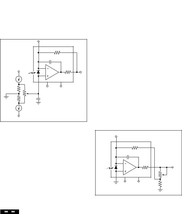
feedback resistors of 100MΩ or greater at room temperature. The dark output voltage can be trimmed to zero with the optional circuit shown in Figure 3.
When used with very large feedback resistors, tiny leakage currents on the circuit board can degrade the performance of the OPT202. Careful circuit board design and clean assembly procedures will help achieve best performance. A “guard ring” on the circuit board can help minimize leakage to the critical non-inverting input (pin 2). This guard ring should encircle pin 2 and connect to Common, pin 8.
|
|
1MΩ |
|
3pF |
|
V+ |
λ |
175Ω |
|
VO |
|
100µA |
|
|
|
OPT202 |
|
1/2 REF200 |
|
|
100Ω |
V+ |
V– |
|
500Ω |
|
100Ω |
0.01µF |
|
100µA |
|
|
1/2 REF200 |
Adjust dark output for 0V. |
|
|
||
|
Trim Range: ±7mV |
|
V– |
|
|
FIGURE 3. Dark Error (Offset) Adjustment Circuit.
LINEARITY PERFORMANCE
Current output of the photodiode is very linear with radiant power throughout a wide range. Nonlinearity remains below approximately 0.01% up to 100μA photodiode current. The photodiode can produce output currents of 10mA or greater with high radiant power, but nonlinearity increases to several percent in this region.
This very linear performance at high radiant power assumes that the full photodiode area is uniformly illuminated. If the light source is focused to a small area of the photodiode, nonlinearity will occur at lower radiant power.
DYNAMIC RESPONSE
Using the internal 1MΩ resistor, the dynamic response of the photodiode/op amp combination can be modeled as a


 ®
®
simple R/C circuit with a –3dB cutoff frequency of 50kHz. This yields a rise time of approximately 10μs (10% to 90%). Dynamic response is not limited by op amp slew rate. This is demonstrated by the dynamic response oscilloscope photographs showing virtually identical large-signal and small-signal response.
Dynamic response will vary with feedback resistor value as shown in the typical performance curve “Voltage Output Responsivity vs Frequency.” Rise time (10% to 90%) will vary according to the –3dB bandwidth produced by a given feedback resistor value—
t |
≈ |
0. 35 |
|
(1) |
f |
|
|||
R |
|
|
|
C
where:
tR is the rise time (10% to 90%) fC is the –3dB bandwidth
NOISE PERFORMANCE
Noise performance of the OPT202 is determined by the op amp characteristics in conjunction with the feedback components and photodiode capacitance. The typical performance curve “Output Noise Voltage vs Measurement Bandwidth” shows how the noise varies with R F and measured bandwidth (1Hz to the indicated frequency). The signal bandwidth of the OPT202 is indicated on the curves. Noise can be reduced by filtering the output with a cutoff frequency equal to the signal bandwidth.
Output noise increases in proportion to the square-root of the feedback resistance, while responsivity increases linearly with feedback resistance. So best signal-to-noise ratio is achieved with large feedback resistance. This comes with the trade-off of decreased bandwidth.
The noise performance of a photodetector is sometimes characterized by Noise Effective Power (NEP). This is the radiant power which would produce an output signal equal to the noise level. NEP has the units of radiant power (watts). The typical performance curve “Noise Effective Power vs Measurement Bandwidth” shows how NEP varies with RF and measurement bandwidth.
|
1MΩ |
RF |
3pF |
|
|
|
|
Gain Adjustment |
|
|
+50%; –0% |
λ |
|
175Ω |
|
VO |
|
|
|
|
|
|
OPT202 |
|
|
5kΩ |
V+ |
V– |
10kΩ |
FIGURE 4. Responsivity (Gain) Adjustment Circuit.
|
OPT202 |
8 |
|
|
1MΩ |
RF |
|
|
|
|
|
|
|
3pF |
|
|
|
|
R1 + R2 |
|
|
|
|
|
|
V |
O |
= |
I |
D |
R |
F |
|
|
|
|
|
R2 |
|
|
|||
|
|
|
|
|
|
|
|
|
|
λ |
|
175Ω |
|
|
|
|
|
|
|
|
|
|
R1 |
|
|
|
|
|
|
|
|
|
|
|
|
|
|
|
|
|
|
OPT202 |
19kΩ |
|
|
|
|
||
V+ |
V– |
|
|
R2 |
|
|
|
|
|
|
|
1kΩ |
|
|
|
|
|||
|
|
|
|
|
|
|
|
||
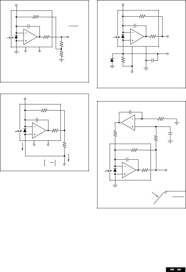
Advantages: High gain with low resistor values.
Less sensitive to circuit board leakage.
Disadvantage: Higher offset and noise than by using high value for RF.
FIGURE 5. “T” Feedback Network.
|
|
1MΩ |
RF |
|
|
|
3pF |
|
|
|
λ |
|
175Ω |
|
|
|
|
+ |
|
|
|
|
OPT202 |
VO = IDRF |
V |
(1) |
|
|
– |
|
|
|
||
Z |
|
|
VZ |
|
|
|
5kΩ |
|
|
3.3V |
|
|
(pesudo-ground) |
|
|
|
|
|
|
|
|
|
0.1µF |
|
|
|
V+ |
|
|
NOTE: (1) Zener diode or other shunt regulator.
FIGURE 7. Single Power Supply Operation.
1MΩ |
RF |
|
||
3pF |
|
|
|
|
λ |
|
175Ω |
|
|
|
|
|
||
|
|
OPT202 |
|
|
ID |
|
|
R1 |
|
–15V |
1kΩ |
|||
+15V |
||||
|
||||
|
|
|
IO ≤ 5mA |
|
IO = ID |
1 + |
RF |
|
|
R1 |
|
|||
|
|
|
||
FIGURE 6. Current Output Circuit.
Other application circuits can be seen in the OPT209 data sheet.
|
C2 |
|
|
0.1µF |
|
|
|
R2 |
|
|
1MΩ |
|
A1 |
|
R3 |
|
C1 |
100kΩ |
|
0.1µF |
|
|
R1 |
|
2 |
1MΩ |
|
|
|
|
1MΩ |
4 |
|
|
|
|
3pF |
|
λ |
175Ω |
5 |
|
||
|
VO |
|
|
|
|
|
OPT202 |
|
|
8 |
|
|
20dB/decade |
|
See AB-061 for details.
f–3dB |
= |
R1 |
|
2πR2R3C2 |
|||
|
|
||
Circuit requires DIP package. |
= 16Hz |
||
FIGURE 8. DC Restoration Rejects Unwanted Steady-State
Background Light.


 ®
®
9 |
OPT202 |
|
|