Материал: 18S20

PRELIMINARY
www.dalsemi.com
FEATURES
Unique 1–Wire® interface requires only one port pin for communication
Multidrop capability simplifies distributed temperature sensing applications
Requires no external components
Can be powered from data line. Power supply range is 3.0V to 5.5V
Zero standby power required
Measures temperatures from –55°C to +125°C. Fahrenheit equivalent is –67°F to +257°F
± 0.5° C accuracy from –10°C to +85°C
Temperature is read as a 9–bit digital value
Converts temperature to digital word in 750 ms (max.)
User–definable, nonvolatile temperature alarm settings
Alarm search command identifies and addresses devices whose temperature is outside of programmed limits (temperature alarm condition)
Software compatible with DS1820 1-Wire digital thermometer
Applications include thermostatic controls, industrial systems, consumer products, thermometers, or any thermally sensitive system
DS18S20
High Precision
1-Wire Digital Thermometer
PIN ASSIGNMENT
DALLAS |
|
|
|
|
|
|
1 |
2 |
3 |
|
|
DS18S20 |
|
|
|||
|
|
|
|
||
1 2 3 |
BOTTOM VIEW |
||||
|
|
|
|
|
|
|
|
DS18S20 To-92 Package |
|
||||||||||
|
|
|
|
|
|
|
|
See Mech Drawings Section |
|||||||||||
|
|
|
|
|
|
|
|
|
|
|
|
|
|
|
|
|
|
|
NC |
|
|
|
|
|
|
|
|
NC |
|
|
|
|
1 |
8 |
|
|
|
|
|
|
GND DQ VDD |
|
|
|
|
|
|
|
|
||||||||||
|
NC |
|
|
|
|
2 |
7 |
|
|
|
|
NC |
|||||||
|
|
|
|
|
|
|
|
|
|
|
|
|
|
|
|
||||
|
|
|
|
|
|
|
VDD |
|
|
|
|
3 |
6 |
|
|
|
|
NC |
|
|
|
|
|
|
|
|
|
||||||||||||
|
|
|
|
|
|
|
|
DQ |
|
|
|
|
4 |
5 |
|
|
|
|
GND |
|
|
|
|
|
|
|
|
|
|
|
|
|
|
|
|||||
|
|
|
|
|
|
|
|
|
|
|
|
|
|
DS18S20Z |
|
||||
|
|
|
|
|
|
|
|
|
|
8-Pin SOIC (150-MIL) |
|
||||||||
PIN DESCRIPTION |
|
|
|
|
|
|
|
|
|
|
|||||||||
GND |
- Ground |
|
|
|
|
|
|
|
|
|
|
|
|
||||||
DQ |
- Data In/Out |
|
|
|
|
|
|
|
|
|
|
|
|
||||||
VDD |
- Power Supply Voltage |
|
|||||||||||||||||
NC |
- No Connect |
|
|
|
|
|
|
|
|
|
|
|
|
||||||
DESCRIPTION
The DS18S20 Digital Thermometer provides 9–bit temperature readings which indicate the temperature of the device.
Information is sent to/from the DS18S20 over a 1–Wire interface, so that only one wire (and ground) needs to be connected from a central microprocessor to a DS18S20. Power for reading, writing, and performing temperature conversions can be derived from the data line itself with no need for an external power source.
Because each DS18S20 contains a unique silicon serial number, multiple DS18S20s can exist on the same 1–Wire bus. This allows for placing temperature sensors in many different places. Applications
1 of 27 |
020100 |

DS18S20
where this feature is useful include HVAC environmental controls, sensing temperatures inside buildings, equipment or machinery, and process monitoring and control.
DETAILED PIN DESCRIPTION
PIN |
PIN |
|
|
8-PIN SOIC |
TO92 |
SYMBOL |
DESCRIPTION |
5 |
1 |
GND |
Ground. |
4 |
2 |
DQ |
Data Input/Output pin. For 1-Wire operation: Open drain. |
|
|
|
(See “Parasite Power” section.) |
3 |
3 |
VDD |
Optional VDD pin. See “Parasite Power” section for details of |
|
|
|
connection. VDD must be grounded for operation in parasite |
|
|
|
power mode. |
DS18S20Z (8-pin SOIC): All pins not specified in this table are not to be connected.
OVERVIEW
The block diagram of Figure 1 shows the major components of the DS18S20. The DS18S20 has three main data components: 1) 64–bit lasered ROM, 2) temperature sensor, 3) nonvolatile temperature alarm triggers TH and TL. The device derives its power from the 1–Wire communication line by storing energy on an internal capacitor during periods of time when the signal line is high and continues to operate off this power source during the low times of the 1–Wire line until it returns high to replenish the parasite (capacitor) supply. As an alternative, the DS18S20 may also be powered from an external 3V - 5V supply.
Communication to the DS18S20 is via a 1–Wire port. With the 1–Wire port, the memory and control functions will not be available before the ROM function protocol has been established. The master must first provide one of five ROM function commands: 1) Read ROM, 2) Match ROM, 3) Search ROM, 4) Skip ROM, or 5) Alarm Search. These commands operate on the 64–bit lasered ROM portion of each device and can single out a specific device if many are present on the 1–Wire line as well as indicate to the bus master how many and what types of devices are present. After a ROM function sequence has been successfully executed, the memory and control functions are accessible and the master may then provide any one of the six memory and control function commands.
One control function command instructs the DS18S20 to perform a temperature measurement. The result of this measurement will be placed in the DS18S20’s scratch-pad memory, and may be read by issuing a memory function command which reads the contents of the scratchpad memory. The temperature alarm triggers TH and TL consist of 1-byte EEPROM each. If the alarm search command is not applied to the DS18S20, these registers may be used as general purpose user memory. Writing TH and TL is done using a memory function command. Read access to these registers is through the scratchpad. All data is read and written least significant bit first.
2 of 27
DS18S20
DS18S20 BLOCK DIAGRAM Figure 1
|
|
|
|
|
|
|
|
|
|
|
|
|
|
|
|
|
|
|
|
|
|
MEMORY AND |
|
|
|
|
|
|
||||||||
|
|
|
|
|
|
|
|
|
|
|
|
|
|
|
|
|
|
|
|
|
|
|
||||||||||||||
|
|
|
|
|
|
|
|
|
|
|
|
|
|
|
|
|
|
|
|
|
|
CONTROL LOGIC |
|
|
|
|
|
|
||||||||
DQ |
|
|
|
|
|
|
|
|
|
|
|
|
|
|
|
|
|
|
|
|
|
|
|
|
|
|
|
|
||||||||
|
|
|
|
|
|
|
|
|
|
|
|
|
|
|
|
|
|
|
|
|
|
|
|
|
|
|
|
|
|
|
|
|
|
|
|
|
|
|
|
|
|
|
|
|
|
|
|
|
|
|
|
|
|
|
|
|
|
|
|
|
|
|
|
|
|
|
|
|
|
|
|
|
|
|
|
|
|
|
|
|
|
|
|
|
|
|
|
|
|
|
|
|
|
|
|
|
|
|
|
|
|
|
|
|
|
|
|
|
|
|
|
|
|
|
|
|
|
|
|
|
|
|
|
|
|
|
|
|
|
|
|
|
|
|
|
|
|
|
|
|
|
|
|
|
|
|
|
|
|
|
|
|
|
|
|
|
INTERNAL VDD |
|
64-BIT ROM |
|
|
|
|
|
|
|
|
|
|
|
|
|
|
|
|
|
TEMPERATURE |
|
|
|
||||
|
|
|
|
|
|
|
|
|
|
AND |
|
|
|
|
|
|
SCRATCHPAD |
|
|
|
|
|
|
|
|
SENSOR |
|
|
|
|||||||
|
|
|
|
|
|
|
|
|
|
|
|
|
|
|
1-WIRE PORT |
|
|
|
|
|
|
|
|
|
|
|
|
|
|
|
|
|
|
|||
|
|
|
|
|
|
|
|
|
|
|
|
|
|
|
|
|
|
|
|
|
|
|
|
|
|
|
|
|
|
|
|
|
|
|
|
|
|
|
|
|
|
|
|
|
|
|
|
|
|
|
|
|
|
|
|
|
|
|
|
|
|
|
|
|
|
|
|
|
|
|
|
|
|
|
|
|
|
|
|
|
|
|
|
|
|
|
|
|
|
|
|
|
|
|
|
|
|
|
|
|
|
|
|
|
|
|
HIGH TEMPERATURE |
|
||
|
|
|
|
|
|
|
|
|
|
|
|
|
|
|
|
|
|
|
|
|
|
|
|
|
|
|
|
|
|
|
|
|
TRIGGER, TH |
|
||
|
|
|
|
|
|
|
|
|
|
|
|
|
|
|
|
|
|
|
|
|
|
|
|
|
|
|
|
|
|
|
|
|
||||
|
|
|
|
|
|
|
|
|
|
|
|
|
|
|
|
|
|
|
|
|
|
|
|
|
|
|
|
|
|
|
|
|
|
|
|
|
|
|
|
|
|
|
|
|
|
|
|
|
|
|
|
|
|
|
|
|
|
|
|
|
|
|
|
|
|
|
|
|
|
|
|
|
|
|
|
|
|
|
|
|
|
|
|
POWER |
|
|
|
|
|
|
|
|
|
|
|
|
|
|
|
|
|
|
|
|
|
|
|
|
||
|
|
|
|
|
|
|
|
|
|
|
|
|
|
|
|
|
|
|
|
|
8-BIT CRC |
|
|
|
|
|
|
|
|
|
LOW TEMPERATURE |
|
|
|||
VDD |
|
|
|
|
|
|
|
|
SUPPLY |
|
|
|
|
|
|
|
|
|
|
|
|
|
|
|
|
|
|
|
|
|
|
|||||
|
|
|
|
|
|
|
|
|
|
|
|
|
|
|
|
|
GENERATOR |
|
|
|
|
|
|
|
|
|
TRIGGER, TH |
|
|
|||||||
|
|
|
|
|
|
|
|
SENSE |
|
|
|
|
|
|
|
|
|
|
|
|
|
|
|
|
|
|
|
|
||||||||
|
|
|
|
|
|
|
|
|
|
|
|
|
|
|
|
|
|
|
|
|
|
|
|
|
|
|
|
|||||||||
|
|
|
|
|
|
|
|
|
|
|
|
|
|
|
|
|
|
|
|
|
|
|
|
|
|
|
|
|
|
|
|
|
|
|
|
|
|
|
|
|
|
|
|
|
|
|
|
|
|
|
|
|
|
|
|
|
|
|
|
|
|
|
|
|
|
|
|
|
|
|
|
|
|
|
|
|
|
|
|
|
|
|
|
|
|
|
|
|
|
|
|
|
|
|
|
|
|
|
|
|
|
|
|
|
|
|
|
|
|
|
PARASITE POWER
The block diagram (Figure 1) shows the parasite-powered circuitry. This circuitry “steals” power whenever the DQ or VDD pins are high. DQ will provide sufficient power as long as the specified timing and voltage requirements are met (see the section titled “1–Wire Bus System”). The advantages of parasite power are twofold: 1) by parasiting off this pin, no local power source is needed for remote sensing of temperature, and 2) the ROM may be read in absence of normal power.
In order for the DS18S20 to be able to perform accurate temperature conversions, sufficient power must be provided over the DQ line when a temperature conversion is taking place. Since the operating current of the DS18S20 is up to 1.5 mA, the DQ line will not have sufficient drive due to the 5K pullup resistor. This problem is particularly acute if several DS18S20s are on the same DQ and attempting to convert simultaneously.
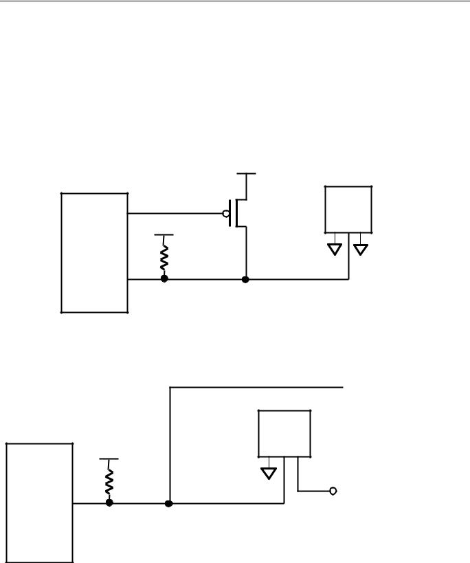
There are two ways to assure that the DS18S20 has sufficient supply current during its active conversion cycle. The first is to provide a strong pullup on the DQ line whenever temperature conversions or copies to the E2 memory are taking place. This may be accomplished by using a MOSFET to pull the DQ line directly to the power supply as shown in Figure 2. The DQ line must be switched over to the strong pull– up within 10 s maximum after issuing any protocol that involves copying to the E2 memory or initiates temperature conversions. When using the parasite power mode, the VDD pin must be tied to ground.
Another method of supplying current to the DS18S20 is through the use of an external power supply tied to the VDD pin, as shown in Figure 3. The advantage to this is that the strong pullup is not required on the DQ line, and the bus master need not be tied up holding that line high during temperature conversions. This allows other data traffic on the 1–Wire bus during the conversion time. In addition, any number of DS18S20s may be placed on the 1–Wire bus, and if they all use external power, they may all simultaneously perform temperature conversions by issuing the Skip ROM command and then issuing the Convert T command. Note that as long as the external power supply is active, the GND pin may not be floating.
The use of parasite power is not recommended above 100° C, since it may not be able to sustain communications given the higher leakage currents the DS18S20 exhibits at these temperatures. For applications in which such temperatures are likely, it is strongly recommended that VDD be applied to the DS18S20.
3 of 27
DS18S20
For situations where the bus master does not know whether the DS18S20s on the bus are parasite powered or supplied with external VDD, a provision is made in the DS18S20 to signal the power supply scheme used. The bus master can determine if any DS18S20s are on the bus which require the strong pullup by sending a Skip ROM protocol, then issuing the read power supply command. After this command is issued, the master then issues read time slots. The DS18S20 will send back “0” on the 1-Wire bus if it is parasite powered; it will send back a “1” if it is powered from the VDD pin. If the master receives a “0,” it knows that it must supply the strong pullup on the DQ line during temperature conversions. See “Memory Command Functions” section for more detail on this command protocol.
STRONG PULL-UP FOR SUPPLYING DS18S20 DURING TEMPERATURE
CONVERSION Figure 2
+3V - +5V
DS18S20
|
+3V - +5V |
|
P |
GND |
VDD |
4.7K |
|
|
|
|
|
|
I/O |
|
USING VDD TO SUPPLY TEMPERATURE CONVERSION CURRENT Figure 3
TO OTHER 1-WIRE DEVICES
DS18S20
|
+3V - +5V |
|
|
|
GND |
VDD |
|
|
4.7K |
EXTERNAL +3V - +5V |
|
|
I/O |
||
P |
SUPPLY |
||
|
|||
|
|
4 of 27

DS18S20
OPERATION – MEASURING TEMPERATURE
The core functionality of the DS18S20 is its direct-to-digital temperature sensor. The direct readout of temperature data is 9 bits wide, equating to a resolution of 0.5° C; if higher resolution is desired, an algorithm is described later in this section to achieve that need. Following the issuance of the Convert T [44h] command, a temperature conversion is performed and the thermal data is stored in the scratchpad memory in a 16-bit, sign-extended two’s complement format. The temperature information can be retrieved over the 1-Wire™ interface by issuing a Read Scratchpad [BEh] command once the conversion has been performed. The data is transferred over the 1-Wire™ bus, LSB first. The MSB of the temperature register contains the “sign” (S) bit, denoting whether the temperature is positive or negative.
Table 2 describes the exact relationship of output data to measured. For Fahrenheit usage, a lookup table or conversion routine must be used.
Temperature/Data Relationships Table 2
|
|
26 |
25 |
24 |
23 |
22 |
21 |
20 |
2-1 |
LSB |
|
|
|
MSb |
(unit = ° C) |
LSb |
|
|
|||||
|
|
|
|
|
|
||||||
|
|
S |
S |
S |
S |
S |
S |
S |
S |
MSB |
|
|
|
|
|
|
|
|
|
|
|
|
|
|
|
|
|
|
|||||||
|
TEMPERATURE |
DIGITAL OUTPUT |
DIGITAL |
|
|||||||
|
|
|
|
|
|
(Binary) |
|
OUTPUT |
|
||
|
|
|
|
|
|
|
|
|
|
(Hex) |
|
|
+85°C |
0000 0101 0101 0000 |
0550h* |
|
|||||||
|
+125°C |
0000 0000 1111 1010 |
00FAh |
|
|||||||
|
+25.0°C |
0000 0000 0011 0010 |
0032h |
|
|||||||
|
+0.5°C |
0000 0000 0000 0001 |
0001h |
|
|||||||
|
|
0°C |
0000 0000 0000 0000 |
0000h |
|
||||||
|
-0.5°C |
1111 1111 1111 1111 |
FFFFh |
|
|||||||
|
-25.0°C |
1111 1111 1100 1110 |
FFCEh |
|
|||||||
|
|
-55°C |
1111 1111 1001 0010 |
FF92h |
|
||||||
|
|
|
|
|
|
|
|
|
|
|
|
*The power on reset register value is +85°C
Higher resolutions may be obtained by the following procedure. First, read the temperature, COUNT_REMAIN, and COUNT_PER_C registers from the scratchpad. Truncate the 0.5° C bit (the LSB) from the temperature value. This value is TEMP_READ. The actual temperature may then be calculated by using the following:
TEMPERATURE = TEMP _ READ − 0.25 + COUNT _ PER _ C − COUNT _ REMAIN COUNT _ PER _ C
OPERATION – ALARM SIGNALING
After the DS18S20 has performed a temperature conversion, the temperature value is compared to the trigger values stored in TH and TL. Since these registers are 8–bit only, the 0.5° C bit is ignored for comparison. The most significant bit of TH or TL directly corresponds to the sign bit of the 16–bit temperature register. If the result of a temperature measurement is higher than TH or lower than TL, an alarm flag inside the device is set. This flag is updated with every temperature measurement. As long as
5 of 27