Материал: 18S20

DS18S20
Example of a ROM Search
The ROM search process is the repetition of a simple three–step routine: read a bit, read the complement of the bit, then write the desired value of that bit. The bus master performs this simple, three–step routine on each bit of the ROM. After one complete pass, the bus master knows the contents of the ROM in one device. The remaining number of devices and their ROM codes may be identified by additional passes.
The following example of the ROM search process assumes four different devices are connected to the same 1–Wire bus. The ROM data of the four devices is as shown:
ROM1 00110101...
ROM2 10101010...
ROM3 11110101...
ROM4 00010001...
The search process is as follows:
1.The bus master begins the initialization sequence by issuing a reset pulse. The slave devices respond by issuing simultaneous presence pulses.
2.The bus master will then issue the Search ROM command on the 1–Wire bus.
3.The bus master reads a bit from the 1–Wire bus. Each device will respond by placing the value of the first bit of their respective ROM data onto the 1–Wire bus. ROM1 and ROM4 will place a 0 onto the 1–Wire bus, i.e., pull it low. ROM2 and ROM3 will place a 1 onto the 1–Wire bus by allowing the line to stay high. The result is the logical AND of all devices on the line, therefore the bus master sees a 0. The bus master reads another bit. Since the Search ROM data command is being executed, all of the devices on the 1–Wire bus respond to this second read by placing the complement of the first bit of their respective ROM data onto the 1–Wire bus. ROM1 and ROM4 will place a 1 onto the 1–Wire, allowing the line to stay high. ROM2 and ROM3 will place a 0 onto the 1–Wire, thus it will be pulled low. The bus master again observes a 0 for the complement of the first ROM data bit. The bus master has determined that there are some devices on the 1–Wire bus that have a 0 in the first position and others that have a 1.
The data obtained from the two reads of the three–step routine have the following interpretations:
00 There are still devices attached which have conflicting bits in this position. 01 All devices still coupled have a 0–bit in this bit position.
10All devices still coupled have a 1–bit in this bit position.
11There are no devices attached to the 1–Wire bus.
4.The bus master writes a 0. This deselects ROM2 and ROM3 for the remainder of this search pass, leaving only ROM1 and ROM4 connected to the 1–Wire bus.
5.The bus master performs two more reads and receives a 0–bit followed by a 1–bit. This indicates that all devices still coupled to the bus have 0s as their second ROM data bit.
6.The bus master then writes a 0 to keep both ROM1 and ROM4 coupled.
7.The bus master executes two reads and receives two 0–bits. This indicates that both 1–bits and 0–bits exist as the third bit of the ROM data of the attached devices.
11 of 27

DS18S20
8.The bus master writes a 0–bit. This deselects ROM1, leaving ROM4 as the only device still connected.
9.The bus master reads the remainder of the ROM bits for ROM4 and continues to access the part if desired. This completes the first pass and uniquely identifies one part on the 1–Wire bus.
10.The bus master starts a new ROM search sequence by repeating steps 1 through 7.
11.The bus master writes a 1–bit. This decouples ROM4, leaving only ROM1 still coupled.
12.The bus master reads the remainder of the ROM bits for ROM1 and communicates to the underlying logic if desired. This completes the second ROM search pass, in which another of the ROMs was found.
13.The bus master starts a new ROM search by repeating steps 1 through 3.
14.The bus master writes a 1–bit. This deselects ROM1 and ROM4 for the remainder of this search pass, leaving only ROM2 and ROM3 coupled to the system.
15.The bus master executes two Read time slots and receives two 0s.
16.The bus master writes a 0–bit. This decouples ROM3, leaving only ROM2.
17.The bus master reads the remainder of the ROM bits for ROM2 and communicates to the underlying logic if desired. This completes the third ROM search pass, in which another of the ROMs was found.
18.The bus master starts a new ROM search by repeating steps 13 through 15.
19.The bus master writes a 1–bit. This decouples ROM2, leaving only ROM3.
20.The bus master reads the remainder of the ROM bits for ROM3 and communicates to the underlying logic if desired. This completes the fourth ROM search pass, in which another of the ROMs was found.
Note the following:
The bus master learns the unique ID number (ROM data pattern) of one 1–Wire device on each ROM Search operation. The time required to derive the part’s unique ROM code is:
960 s + (8 + 3 x 64) 61 s = 13.16 ms
The bus master is therefore capable of identifying 75 different 1–Wire devices per second.
I/O SIGNALING
The DS18S20 requires strict protocols to insure data integrity. The protocol consists of several types of signaling on one line: reset pulse, presence pulse, write 0, write 1, read 0, and read 1. All of these signals, with the exception of the presence pulse, are initiated by the bus master.
12 of 27

DS18S20
The initialization sequence required to begin any communication with the DS18S20 is shown in Figure 10. A reset pulse followed by a presence pulse indicates the DS18S20 is ready to send or receive data given the correct ROM command and memory function command.
The bus master transmits (TX) a reset pulse (a low signal for a minimum of 480 ms). The bus master then releases the line and goes into a receive mode (RX). The 1–Wire bus is pulled to a high state via the 5K pullup resistor. After detecting the rising edge on the DQ pin, the DS18S20 waits 15–60 s and then transmits the presence pulse (a low signal for 60–240 s).
MEMORY COMMAND FUNCTIONS
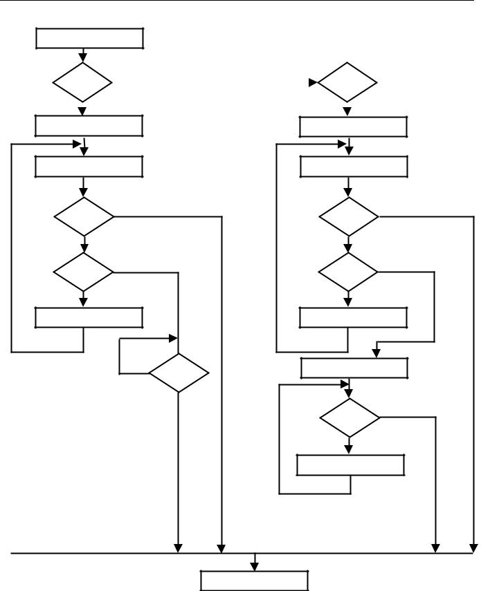
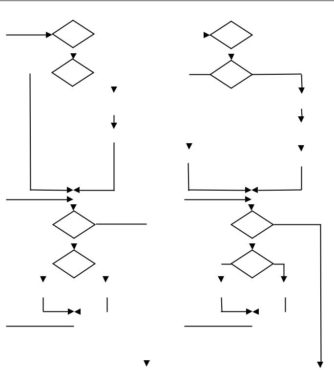
The following command protocols are summarized in Table 2, and by the flowchart of Figure 9.
Write Scratchpad [4Eh]
This command writes to the scratchpad of the DS18S20, starting at the TH register. The next 2 bytes written will be saved in scratchpad memory at address locations 2 and 3. Writing may be terminated at any point by issuing a reset.
Read Scratchpad [BEh]
This command reads the contents of the scratchpad. Reading will commence at byte 0, and will continue through the scratchpad until the 9th (byte 8, CRC) byte is read. If not all locations are to be read, the master may issue a reset to terminate reading at any time.
Copy Scratchpad [48h]
This command copies the scratchpad into the E2 memory of the DS18S20, storing the temperature trigger bytes in nonvolatile memory. If the bus master issues read time slots following this command, the DS18S20 will output 0 on the bus as long as it is busy copying the scratchpad to E2; it will return a 1 when the copy process is complete. If parasite-powered, the bus master has to enable a strong pullup for at least 10 ms immediately after issuing this command.
Convert T [44h]
This command begins a temperature conversion. No further data is required. The temperature conversion will be performed and then the DS18S20 will remain idle. If the bus master issues read time slots following this command, the DS18S20 will output 0 on the bus as long as it is busy making a temperature conversion; it will return a 1 when the temperature conversion is complete. If parasite-powered, the bus master has to enable a strong pullup for a time period greater than tconv immediately after issuing this command.
Recall E2 [B8h]
This command recalls the temperature trigger values stored in E2 to the scratchpad. This recall operation happens automatically upon power–up to the DS18S20 as well, so valid data is available in the scratchpad as soon as the device has power applied. With every read data time slot issued after this command has been sent, the device will output its temperature converter busy flag: 0=busy, 1=ready.
Read Power Supply [B4h]
With every read data time slot issued after this command has been sent to the DS18S20, the device will signal its power mode: 0=parasite power, 1=external power supply provided.
13 of 27
DS18S20
MEMORY FUNCTIONS FLOW CHART Figure 9
MASTER TX MEMORY OR
CONTROL COMMAND
4Eh |
N |
BEh |
N |
|||
WRITE |
|
READ |
|
|||
SCRATCHPAD |
|
SCRATCHPAD |
|
|||
? |
|
? |
|
|
||
|
|
Y |
|
|
Y |
|
|
|
|
|
|||
DS18S20 SETS ADDRESS
COUNTER TO 2
DS18S20 SETS ADDRESS
COUNTER TO 0
MASTER TX DATA BYTE |
MASTER RX DATA |
|
|
TO SCRATCHPAD |
|
FROM SCRATCHPAD |
|
|
|
Y |
Y |
MASTER |
|
MASTER |
|
|
|
||
TX RESET |
|
TX RESET |
|
? |
|
? |
|
N |
|
N |
|
ADDRESS |
Y |
ADDRESS |
Y |
=3 |
|
=7 |
|
? |
|
? |
|
N |
|
N |
|
DS18S20 INCREMENTS |
|
DS18S20 TX |
|
|
DS18S20 INCREMENTS |
|
|
ADDRESS |
|
SERIAL NUMBER |
|
|
ADDRESS |
|
|
|
|
6 BYTES |
|
N |
MASTER |
MASTER RX 8-BIT |
|
CRC OF DATA |
|
||
|
TX RESET |
|
|
|
|
|
|
|
? |
|
|
|
Y |
|
Y |
|
|
MASTER |
|
|
|
|
|
|
|
TX RESET |
|
|
|
? |
|
|
|
N |
|
|
|
MASTER RX “1s” |
|
DS18S20 TX
PRESENCE PULSE
14 of 27
DS18S20
MEMORY FUNCTIONS FLOW CHART Figure 9 (cont’d)
|
48h |
|
N |
|
|
44h |
N |
||||||||||||
|
COPY |
|
|
|
|||||||||||||||
|
|
|
|
|
|
|
|
|
|
|
CONVERT |
|
|
|
|||||
|
SCRATCHPAD |
|
|
|
|
|
|
|
|
|
|
|
|
|
|||||
|
|
|
|
|
|
|
|
|
|
TEMPERATURE |
|
|
|
||||||
|
|
|
|
|
|
|
|
|
|
|
|
|
|||||||
|
? |
|
|
|
|
|
|
|
|
|
|
|
|
|
|||||
|
|
|
|
|
|
|
|
|
|
|
|
|
|
|
|
|
|
||
|
|
|
Y |
|
|
|
|
|
|
|
|
|
|
|
|
Y |
|
|
|
|
|
|
|
|
|
|
|
|
|
|
|
|
|
|
|
|
|
||
N |
PARASITE |
|
Y |
|
PARASITE |
Y |
|||||||||||||
|
POWER |
|
|
|
|
|
|
|
N |
|
|||||||||
|
? |
|
|
|
|
|
|
|
|
|
|
|
POWER |
|
|
|
|||
|
|
|
|
|
|
|
|
|
|
|
? |
|
|
|
|
||||
|
|
|
|
|
|
|
|
|
|
|
|
|
|
|
|
|
|||
|
|
|
|
|
|
|
|
|
|
|
|
|
|
|
|
|
|
|
|
|
|
|
|
|
|
|
|
|
|
|
|
|
|
|
|
|
|
||
|
|
|
|
|
MASTER ENABLES |
|
|
|
|
|
|
|
|
|
|
|
MASTER ENABLES |
||
|
|
|
|
STRONG PULLUP FOR |
|
|
|
|
|
|
|
|
|
|
STRONG PULL-UP |
||||
|
|
|
|
|
10ms |
|
|
|
|
|
|
|
|
|
|
|
|
|
|
|
|
|
|
|
|
|
|
|
|
|
|
|
|
|
|
|
|
||
|
|
|
|
|
|
|
|
|
|
|
|
|
|
|
|
|
|
|
|
|
|
|
|
|
|
|
|
|
|
|
|
|
|
|
|
|
|
|
|
|
|
|
|
|
|
|
|
|
|
|
|
|
|
|
|
|
|
DS18S20 CONVERTS |
|
|
|
|
|
|
MASTER DISABLES |
|
|
|
|
|
|
|
|
|
|
TEMPERATURE |
|||
|
|
|
|
|
|
|
|
|
|
|
|
|
|
|
|
|
|||
|
|
|
|
|
STRONG PULLUP |
|
|
|
|
|
|
|
|
|
|
|
|
||
|
|
|
|
|
|
|
|
|
|
|
|
|
|
|
|
|
|
|
|
|
|
|
|
|
|
|
|
|
|
|
|
|
|
|
|
|
|
|
|
|
|
|
|
|
|
|
|
|
|
DS18S20 BEGINS |
|
|
|
|
|
MASTER DISABLES |
|||
|
|
|
|
|
|
|
|
|
|
CONVERSION |
|
|
|
|
|
STRONG PULL-UP |
|||
|
|
|
|
|
|
|
|
|
|
|
|
|
|
|
|
|
|
|
|
|
|
|
|
|
|
|
|
|
Y |
|
|
|
|
|
|
|
|
|
|
Y |
|
|||||||
|
|
|
|
|
|
|
|
|
|
|
|
|
|
|
|
|
|
|
|
|||||||||
|
|
|
|
|
|
|
|
|
|
|
|
|
|
|
|
|
|
|
|
|||||||||
|
|
|
|
MASTER TX |
|
|
|
|
|
|
|
|
|
|
|
MASTER TX |
|
|
|
|
||||||||
|
|
|
|
RESET |
|
|
|
|
|
|
|
|
|
|
|
RESET |
|
|
|
|
||||||||
|
|
|
? |
|
|
|
|
|
|
|
|
|
|
|
|
? |
|
|
|
|
|
|
||||||
|
|
|
|
|
|
N |
|
|
|
|
|
|
|
|
|
|
|
|
|
N |
|
|
|
|
||||
|
|
|
|
|
|
|
|
|
|
|
|
|
|
|
|
|
|
|
|
|
|
|
||||||
|
|
N |
NONVOLATILE |
Y |
|
|
|
|
N |
DEVICE BUSY |
Y |
|
||||||||||||||||
|
|
|
|
MEMORY |
|
|
|
|
|
|
|
|
|
|
CONVERTING |
|
|
|
|
|||||||||
|
|
|
|
|
|
|
|
|
|
|
|
|
|
|
|
|
|
|||||||||||
|
|
|
|
BUSY |
|
|
|
|
|
|
|
|
|
|
TEMPERATURE |
|
|
|
|
|||||||||
|
|
|
? |
|
|
|
|
|
|
|
|
|
|
|
|
? |
|
|
|
|
|
|
||||||
|
|
|
|
|
|
|
|
|
|
|
|
|
|
|
|
|
|
|
|
|
|
|
|
|
|
|
|
|
|
MASTER |
|
|
|
|
|
|
MASTER |
|
|
|
|
|
|
|
|
|
|
|
|
|
MASTER |
|
|
||||
|
|
|
|
|
|
|
MASTER |
|
|
|
|
|
|
|
||||||||||||||
|
RX “1”S |
|
|
|
|
|
|
RX “0”S |
|
|
|
|
|
RX “1”S |
|
|
|
|
|
|
RX “0”S |
|
|
|||||
|
|
|
|
|
|
|
|
|
|
|
|
|
|
|
|
|
|
|
|
|
|
|
|
|
|
|
|
|
|
|
|
|
|
|
|
|
|
|
|
|
|
|
|
|
|
|
|
|
|
|
|
|
|
|
|
|
|
|
|
|
|
|
|
|
|
|
|
|
|
|
|
|
|
|
|
|
|
|
|
|
|
|
|
|
|
|
|
|
|
|
|
|
|
|
|
|
|
|
|
|
|
|
|
|
|
|
|
|
|
|
|
|
|
|
|
|
|
|
|
|
|
|
|
|
|
|
|
|
|
|
|
|
|
|
|
|
|
|
|
|
|
|
|
|
15 of 27