Материал: 18S20
DS18S20
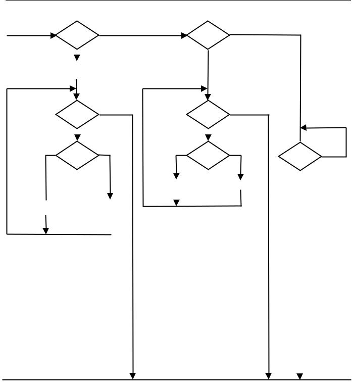
MEMORY FUNCTIONS FLOW CHART Figure 9 (cont’d)
|
B8h |
N |
B4h |
N |
|
|
READ |
||||
|
RECALL |
|
|
||
|
E2 |
|
POWERSUPPLY |
|
|
? |
|
? |
|
||
|
|
Y |
|
Y |
|
|
|
|
|
||
|
|
|
|
|
|
|
|
|
|
|
|
|
DS18S20 RECALLS |
|
|
|
|
|
FROM E2 PROM |
|
|
|
|
|
|
|
|
|
|
|
|
|
|
|
|
Y |
|
|
|
|
|
Y |
|
|
|
|
|
|
|
MASTER TX |
|
|
|
|
|
MASTER TX |
|
|
|
|
|||
|
|
|
RESET |
|
|
|
|
|
RESET |
|
|
|
|
|||
|
? |
|
|
|
|
|
|
? |
|
|
|
|
||||
|
|
|
|
N |
|
|
|
|
|
|
N |
|
|
|
|
|
|
|
|
|
|
|
|
|
|
|
|
|
|
|
|||
N |
|
|
DEVICE |
Y |
|
|
N |
PARASITE |
Y |
MASTER |
N |
|||||
|
BUSY CONVERTING |
|
|
|
|
|
POWERED |
|
TX RESET |
|
||||||
|
|
TEMPERATURE |
|
|
|
|
|
|
|
|||||||
|
|
|
|
|
|
|
? |
|
? |
|
|
|||||
|
? |
|
|
|
|
|
|
|
|
|
||||||
|
|
|
|
|
|
|
|
|
|
|
|
|
||||
|
|
|
|
|
|
|
|
|
|
|
|
|
|
|
Y |
|
|
|
|
|
|
|
|
|
|
|
|
|
|
|
|
|
|
|
|
|
|
|
|
|
|
|
MASTER |
|
|
MASTER |
|
|
|
|
|
|
|
|
|
|
|
|
|
RX “1”S |
|
|
RX “0”S |
|
|
|
|
|
|
|
|
|
|
|
|
|
|
|
|
|
|
|
|
|
|
|
|
|
|
|
|
|
|
|
|
|
|
|
|
|
|
MASTER |
|
|
|
|
|
MASTER |
|
|
|
|
|
|
|
|
|
|
RX “1”S |
|
|
|
|
|
RX “0”S |
|
|
|
|
|
|
|
|
|
|
|
|
|
|
|
|
|
|
|
|
|
|
|
|
|
|
|
|
|
|
|
|
|
|
|
|
|
|
|
|
|
|
|
|
|
|
|
|
|
|
|
|
|
|
|
|
|
|
|
|
|
16 of 27
DS18S20
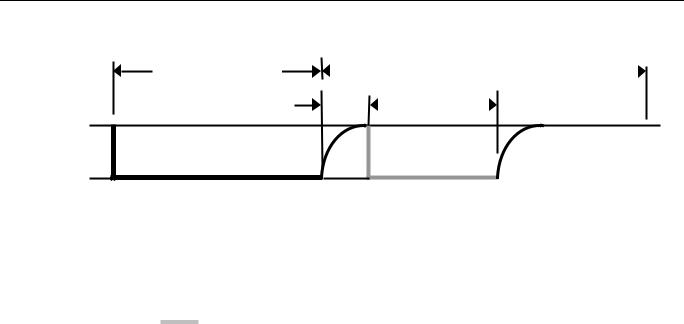
INITIALIZATION PROCEDURE “RESET AND PRESENCE PULSES” Figure 10
Master TX "reset pulse" 480 s minmum 960 s maximum
VCC
1-WIRE
BUS
GND
|
|
|
|
|
Master RX |
||||||
|
|
|
|
480 s minmum |
|
|
|
||||
DS18S20 TX |
|
|
|
||||||||
|
DS18S20 TX |
||||||||||
|
waits |
"presence Pulse" |
|||||||||
15-60 s |
|
60-240 s |
|
|
|
|
|||||
|
|
||||||||||
|
|
|
|
|
|
|
|
|
|
|
|
|
|
|
|
|
|
|
|
|
|
|
|
|
LINE TYPE LEGEND |
|
|
||
|
|
|
Bus master active low |
|
DS18S20 active low |
|
|
|
|||
|
|
|
Both bus master and |
|
Resistor pull-up |
|
|
|
DS18S20 active low |
|
|
|
|
|
|
|
|
DS18S20 COMMAND SET Table 2
|
|
|
1-WIRE BUS |
|
|
|
|
AFTER ISSUING |
|
INSTRUCTION |
DESCRIPTION |
PROTOCOL |
PROTOCOL |
NOTES |
|
TEMPERATURE CONVERSION COMMANDS |
|
||
Convert T |
Initiates temperature |
44h |
<read temperature busy |
1 |
|
conversion. |
|
status> |
|
|
MEMORY COMMANDS |
|
|
|
Read Scratchpad |
Reads bytes from |
BEh |
<read data up to 9 bytes> |
|
|
scratchpad and reads |
|
|
|
|
CRC byte. |
|
|
|
Write Scratchpad |
Writes bytes into |
4Eh |
<write data into 2 bytes |
|
|
scratchpad at addresses 2 |
|
at addr. 2 and addr 3> |
|
|
and 3 (TH and TL |
|
|
|
|
temperature triggers). |
|
|
|
Copy Scratchpad |
Copies scratchpad into |
48h |
<read copy status> |
2 |
|
nonvolatile memory |
|
|
|
|
(addresses 2 and 3 only). |
|
|
|
Recall E2 |
Recalls values stored in |
B8h |
<read temperature busy |
|
|
nonvolatile memory into |
|
status> |
|
|
scratchpad (temperature |
|
|
|
|
triggers). |
|
|
|
Read Power Supply |
Signals the mode of |
B4h |
<read supply status> |
|
|
DS18S20 power supply |
|
|
|
|
to the master. |
|
|
|
17 of 27

DS18S20
NOTES:
1.Temperature conversion takes up to 750 ms. After receiving the Convert T protocol, if the part does
not receive power from the VDD pin, the DQ line for the DS18S20 must be held high for at least 750 ms to provide power during the conversion process. As such, no other activity may take place on the 1–Wire bus for at least this period after a Convert T command has been issued.
2.After receiving the Copy Scratchpad protocol, if the part does not receive power from the VDD pin, the DQ line for the DS18S20 must be held high for at least 10 ms to provide power during the copy process. As such, no other activity may take place on the 1–Wire bus for at least this period after a Copy Scratchpad command has been issued.
READ/WRITE TIME SLOTS
DS18S20 data is read and written through the use of time slots to manipulate bits and a command word to specify the transaction.
Write Time Slots
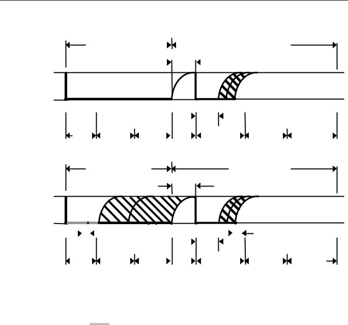
A write time slot is initiated when the host pulls the data line from a high logic level to a low logic level. There are two types of write time slots: Write 1 time slots and Write 0 time slots. All write time slots must be a minimum of 60 s in duration with a minimum of a 1- s recovery time between individual write cycles.
The DS18S20 samples the DQ line in a window of 15 s to 60 s after the DQ line falls. If the line is high, a Write 1 occurs. If the line is low, a Write 0 occurs (see Figure 11).
For the host to generate a Write 1 time slot, the data line must be pulled to a logic low level and then released, allowing the data line to pull up to a high level within 15 s after the start of the write time slot.
For the host to generate a Write 0 time slot, the data line must be pulled to a logic low level and remain low for 60 s.
Read Time Slots
The host generates read time slots when data is to be read from the DS18S20. A read time slot is initiated when the host pulls the data line from a logic high level to logic low level. The data line must remain at a low logic level for a minimum of 1 s; output data from the DS18S20 is valid for 15 s after the falling edge of the read time slot. The host therefore must stop driving the DQ pin low in order to read its state 15 s from the start of the read slot (see Figure 11). By the end of the read time slot, the DQ pin will pull back high via the external pullup resistor. All read time slots must be a minimum of 60 s in duration with a minimum of a 1- s recovery time between individual read slots.
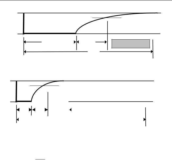
Figure 12 shows that the sum of TINIT, TRC, and TSAMPLE must be less than 15 s. Figure 13 shows that system timing margin is maximized by keeping TINIT and TRC as small as possible and by locating the
master sample time towards the end of the 15- s period.
18 of 27
DS18S20
READ/WRITE TIMING DIAGRAM Figure 11
Master Write "0" Slot |
|
|
|
|
|
|
|
|
|
|
|
|
|
|
|
Master Write "1" Slot |
|
60 s <Tx "0" < 120 s |
|
|
|
|
|
|
|
|
|
|
|
|
|
||||
|
|
|
1 s < tREC < ∞ |
|||||
|
|
|||||||
|
|
|
|
|
|
|
|
|
VCC
1-WIRE
BUS
GND
|
|
|
|
|
DS18S20 SAMPLES |
|
|
|
|
|
>1 s |
|
|
|
|
|
|
DS18S20 SAMPLES |
|
||||||||||||
|
|
|
|
MIN |
TYP |
|
MAX |
|
|
|
|
|
|
|
|
|
|
|
|
|
MIN |
TYP |
MAX |
|
|||||||
|
|
|
|
|
|
|
|
|
|
|
|
|
|
|
|
|
|
|
|
|
|
|
|
|
|
|
|
|
|
|
|
15 s |
|
|
|
|
15 s |
|
|
|
|
30 s |
|
|
|
|
|
|
15 s |
|
|
|
|
15 s |
|
|
|
|
30 s |
|
|||
|
|
|
|
|
|
|
|
|
|
|
|
|
|
|
|
|
|
|
|
|
|||||||||||
|
|
|
|
|
|
|
|
|
|
|
|
|
|
|
|
|
|
|
|
||||||||||||
|
|
|
|
|
|
|
|
|
|
|
|
|
|
|
|
|
|
|
|
|
|
Master Read "1" Slot |
|
|
|||||||
|
|
|
Master Read "0" Slot |
|
|
|
|
|
|
|
|
|
|
|
|
|
|
||||||||||||||
|
|
|
|
|
|
|
|
|
|
|
|
|
1 s < tREC < ∞ |
|
|
|
|
|
|
|
|
|
|
|
|||||||
|
|
|
|
|
|
|
|
|
|
|
|
|
|
|
|
|
|
|
|
|
|
|
|
||||||||
VCC
1-WIRE
BUS
GND
|
|
|
|
|
|
|
|
|
|
Master Samples |
|
|
|
|
|
|
|
|
|
|
|
|
Master Samples |
|||||||||||
|
|
|
|
|
|
|
|
|
|
|
|
|
|
|
|
|
|
|
>1 s |
|
|
|
|
|
|
|
|
|
|
|
|
|||
|
|
|
|
|
|
|
|
|
|
|
|
|
|
|
|
|
|
|
|
|
|
|
|
|
|
|
|
|
|
|||||
|
|
|
|
|
|
|
|
|
|
|
|
|
|
|
|
|
|
|
|
|
|
|
|
|
|
|
|
|
|
|
|
|
|
|
|
|
15 s |
|
|
|
|
|
15 s |
|
|
|
30 s |
|
|
|
|
|
|
15 s |
|
|
|
|
|
|
|
|
|
30 s |
|||||
|
|
|
|
|
|
|
|
|
|
|
|
|
||||||||||||||||||||||
|
|
|
|
|
|
|
|
|
|
|
|
|
|
|
|
|
|
|
|
|
|
|
|
|
|
|
|
|||||||
|
|
|
|
|
LINE TYPE LEGEND |
|
|
|
|
|
|
|
|
|
|
|
|
|
|
|
|
|
|
|
|
|
||||||||
|
|
|
|
|
|
|
|
|
|
Bus master active low |
|
|
|
|
|
|
|
|
|
DS18S20 active low |
|
|||||||||||||
|
|
|
|
|
|
|
|
|
|
|
|
|
|
|
|
|
|
|
|
|||||||||||||||
|
|
|
|
|
|
|
|
|
|
Both bus master and |
|
|
|
|
|
|
|
|
|
Resistor pull-up |
|
|||||||||||||
|
|
|
|
|
|
|
|
|
|
DS18S20 active low |
|
|
|
|
|
|
|
|
|
|
|
|
|
|
|
|
|
|
||||||
|
|
|
|
|
|
|
|
|
|
|
|
|
|
|
|
|
|
|
|
|
|
|
|
|
|
|
|
|
|
|
|
|
|
|
19 of 27
DS18S20
DETAILED MASTER READ 1 TIMING Figure 12
VCC
VIH OF MASTER
1-WIRE
BUS
GND
TINIT > 1 s |
|
|
|
TRC |
|
|
MASTER SAMPLES
15 s
RECOMMENDED MASTER READ 1 TIMING Figure 13
VCC
VIH OF MASTER
1-WIRE
BUS
GND
|
|
|
|
|
|
|
|
|
|
|
TINIT = |
|
TRC = |
|
|
|
MASTER SAMPLES |
|
|
|
SMALL |
|
SMALL |
|
|
|
|
|
|
|
|
|
|
|
|
15 s |
|
|
|
|
LINE TYPE LEGEND |
|
|
|
|
|
Bus master active low |
|
DS18S20 active low |
|
|
|
||
|
|
Both bus master and |
|
Resistor pull-up |
|
|
DS18S20 active low |
|
|
|
|
|
|
|
20 of 27