Материал: 18S20

DS18S20
the alarm flag is set, the DS18S20 will respond to the alarm search command. This allows many DS18S20s to be connected in parallel doing simultaneous temperature measurements. If somewhere the temperature exceeds the limits, the alarming device(s) can be identified and read immediately without having to read non–alarming devices.
64-BIT LASERED ROM
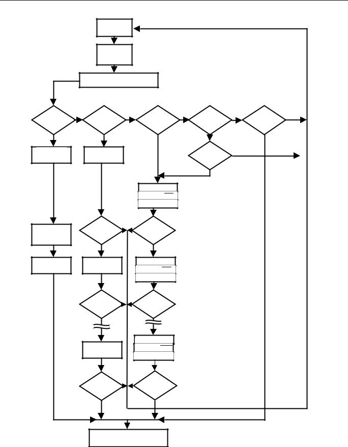
Each DS18S20 contains a unique ROM code that is 64–bits long. The first 8 bits are a 1–Wire family code (DS18S20 code is 10h). The next 48 bits are a unique serial number. The last 8 bits are a CRC of the first 56 bits. (See Figure 4.) The 64–bit ROM and ROM Function Control section allow the DS18S20 to operate as a 1–Wire device and follow the 1–Wire protocol detailed in the section “1–Wire Bus System.” The functions required to control sections of the DS18S20 are not accessible until the ROM function protocol has been satisfied. This protocol is described in the ROM function protocol flowchart (Figure 5). The 1–Wire bus master must first provide one of five ROM function commands: 1) Read ROM, 2) Match ROM, 3) Search ROM, 4) Skip ROM, or 5) Alarm Search. After a ROM functions sequence has been successfully executed, the functions specific to the DS18S20 are accessible and the bus master may then provide one of the six memory and control function commands.
CRC GENERATION
The DS18S20 has an 8–bit CRC stored in the most significant byte of the 64–bit ROM. The bus master can compute a CRC value from the first 56–bits of the 64–bit ROM and compare it to the value stored within the DS18S20 to determine if the ROM data has been received error–free by the bus master. The equivalent polynomial function of this CRC is:
CRC = X8 + X5 + X4 + 1
The DS18S20 also generates an 8–bit CRC value using the same polynomial function shown above and provides this value to the bus master to validate the transfer of data bytes. In each case where a CRC is used for data transfer validation, the bus master must calculate a CRC value using the polynomial function given above and compare the calculated value to either the 8–bit CRC value stored in the 64–bit ROM portion of the DS18S20 (for ROM reads) or the 8–bit CRC value computed within the DS18S20 (which is read as a ninth byte when the scratchpad is read). The comparison of CRC values and decision to continue with an operation are determined entirely by the bus master. There is no circuitry inside the DS18S20 that prevents a command sequence from proceeding if the CRC stored in or calculated by the DS18S20 does not match the value generated by the bus master.
The 1–Wire CRC can be generated using a polynomial generator consisting of a shift register and XOR gates as shown in Figure 6. Additional information about the Dallas 1–Wire Cyclic Redundancy Check is available in Application Note 27 entitled “Understanding and Using Cyclic Redundancy Checks with Dallas Semiconductor Touch Memory Products.”
The shift register bits are initialized to “0”. Then starting with the least significant bit of the family code, one bit at a time is shifted in. After the eighth bit of the family code has been entered, then the serial number is entered. After the 48th bit of the serial number has been entered, the shift register contains the CRC value. Shifting in the 8 bits of CRC should return the shift register to all “0s”.
64-BIT LASERED ROM Figure 4
8-BIT CRC CODE |
|
48-BIT SERIAL NUMBER |
8-BIT FAMILY CODE (10h) |
||
MSB |
LSB MSB |
LSB |
MSB |
LSB |
|
6 of 27
DS18S20
ROM FUNCTIONS FLOW CHART Figure 5 |
|
|
|
|
|||||
|
|
MASTER TX |
|
|
|
|
|
|
|
|
|
RESET PULSE |
|
|
|
|
|
|
|
|
|
DS18S20 TX |
|
|
|
|
|
|
|
|
|
PRESENCE |
|
|
|
|
|
|
|
|
|
PULSE |
|
|
|
|
|
|
|
|
|
MASTER TX ROM |
|
|
|
|
|
||
|
|
FUNCTION COMMAND |
|
|
|
|
|
||
33h |
N |
55h |
N |
F0h |
N |
ECh |
N |
CCh |
N |
ALARM |
|||||||||
READ ROM |
|
MATCH ROM |
|
SEARCH ROM |
|
SEARCH |
|
SKIP ROM |
|
COMMAND |
|
COMMAND |
|
COMMAND |
|
COMMAND |
|
COMMAND |
|
Y |
|
Y |
|
Y |
|
Y |
|
Y |
|
DS18S20 TX |
|
MASTER TX |
|
|
|
ALARM |
N |
|
|
FAMILY CODE |
|
|
|
|
|
|
|
||
|
BIT 0 |
|
|
|
|
|
|
||
1 BYTE |
|
|
|
|
CONDITION ? |
|
|
|
|
|
|
|
|
|
|
|
|
||
|
|
|
|
|
|
Y |
|
|
|
|
|
|
|
DS18S20 TX BIT 0 |
|
|
|
|
|
|
|
|
|
DS18S20 TX BIT 0 |
|
|
|
|
|
|
|
|
|
MASTER TX BIT 0 |
|
|
|
|
|
|
|
|
N |
N |
|
|
|
|
|
DS18S20 TX |
|
BIT 0 |
|
BIT 0 |
|
|
|
|
|
SERIAL NUMBER |
|
MATCH? |
|
MATCH? |
|
|
|
|
|
6 BYTES |
|
|
|
|
|
|
|
|
|
|
|
Y |
|
Y |
|
|
|
|
|
DS18S20 TX |
|
MASTER TX |
|
DS18S20 TX BIT 1 |
|
|
|
|
|
|
|
|
|
|
|
|
|
||
CRC BYTE |
|
BIT 1 |
|
DS18S20 TX BIT 1 |
|
|
|
|
|
|
|
|
|
|
|
|
|
||
|
|
|
|
MASTER TX BIT 1 |
|
|
|
|
|
|
|
N |
|
N |
|
|
|
|
|
|
|
BIT 1 |
|
BIT 1 |
|
|
|
|
|
|
|
MATCH? |
|
MATCH? |
|
|
|
|
|
|
|
Y |
|
Y |
|
|
|
|
|
|
|
|
|
|
|
|
|
|
|
|
|
|
|
DS18S20 TX BIT 63 |
|
|
|
|
|
|
|
MASTER TX |
|
DS18S20 TX BIT 63 |
|
|
|
|
|
|
|
BIT 63 |
|
MASTER TX BIT 63 |
|
|
|
|
|
|
|
|
|
|
|
|
|
|
|
|
|
N |
|
N |
|
|
|
|
|
|
|
BIT 63 |
|
BIT 63 |
|
|
|
|
|
|
|
MATCH? |
|
MATCH? |
|
|
|
|
|
|
|
Y |
|
Y |
|
|
|
|
|
|
|
|
|
|
|
|
|
|
|
|
|
MASTER TX MEMORY OR CONTROL |
|
|
|
|
|
||
|
|
FUNCTION COMMAND |
|
|
|
|
|
||
7 of 27

DS18S20
1-WIRE CRC CODE Figure 6
|
|
INPUT |
XOR |
XOR |
XOR |
(MSB) |
|
(LSB) |
MEMORY
The DS18S20’s memory is organized as shown in Figure 7. The memory consists of a scratchpad RAM and a nonvolatile, electrically erasable (E2) RAM, which stores the high and low temperature triggers, TH and TL. The scratchpad helps insure data integrity when communicating over the 1–Wire bus. Data is first written to the scratchpad where it can be read back. After the data has been verified, a copy scratchpad command will transfer the data to the nonvolatile (E2) RAM. This process insures data integrity when modifying the memory. The scratchpad is organized as 8 bytes of memory. The first 2-bytes contain the measured temperature information. The third and fourth bytes are volatile copies of TH and TL and are refreshed with every power–on reset. The next 2 bytes are not used; upon reading back, however, they will appear as all logic “1s”. The seventh and eighth bytes are count registers, which may be used in obtaining higher temperature resolution (see “Operation–measuring Temperature” section). There is a ninth byte which may be read with a Read Scratchpad command. This byte contains a cyclic redundancy check (CRC) byte which is the CRC over all of the 8 previous bytes. This CRC is implemented in the fashion described in the section titled “CRC Generation."
DS18S20 MEMORY MAP Figure 7
|
SCRATCHPAD |
|
BYTE |
E2 RAM |
|
TEMPERATURE LSB |
|
|
|||
|
0 |
|
|||
|
|
|
|
|
|
TEMPERATURE MSB |
|
1 |
|
||
|
|
|
|
|
|
|
TH/USER BYTE 1 |
2 |
TH/USER BYTE 1 |
||
|
|
|
|
|
|
|
TL/USER BYTE 2 |
3 |
TL/USER BYTE 2 |
||
|
|
|
|
|
|
|
RESERVED |
|
4 |
|
|
|
|
|
|
|
|
|
RESERVED |
|
5 |
|
|
|
|
|
|
|
|
|
|
|
|
|
|
|
COUNT REMAIN |
|
6 |
|
|
|
|
|
|
|
|
|
|
|
|
|
|
|
COUNT PER °C |
|
7 |
|
|
|
|
|
|
|
|
|
|
|
|
||
|
CRC |
8 |
|
||
|
|
|
|
|
|
8 of 27
DS18S20
1-WIRE BUS SYSTEM
The 1–Wire bus is a system which has a single bus master and one or more slaves. The DS18S20 behaves as a slave. The discussion of this bus system is broken down into three topics: hardware configuration, transaction sequence, and 1–Wire signaling (signal types and timing).
HARDWARE CONFIGURATION
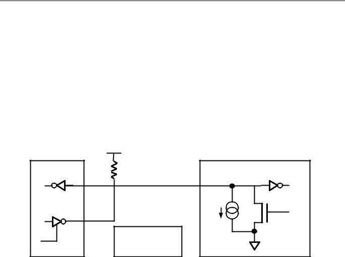
The 1–Wire bus has only a single line by definition; it is important that each device on the bus be able to drive it at the appropriate time. To facilitate this, each device attached to the 1–Wire bus must have open drain or 3–state outputs. The 1–Wire port of the DS18S20 (DQ pin) is open drain with an internal circuit equivalent to that shown in Figure 8. A multidrop bus consists of a 1–Wire bus with multiple slaves attached. The 1–Wire bus requires a pullup resistor of approximately 5KΩ .
HARDWARE CONFIGURATION Figure 8
|
+3V - +5V |
BUS MASTER |
DS18S20 1-WIRE PORT |
|
4.7K |
RX |
RX |
|
5 µA |
TX |
Typ. |
|
TX |
100 OHM |
RX = RECEIVE |
MOSFET |
|
|
TX = TRANSMIT |
|
The idle state for the 1–Wire bus is high. If for any reason a transaction needs to be suspended, the bus MUST be left in the idle state if the transaction is to resume. Infinite recovery time can occur between bits so long as the 1–Wire bus is in the inactive (high) state during the recovery period. If this does not occur and the bus is left low for more than 480 µ s, all components on the bus will be reset.
TRANSACTION SEQUENCE
The protocol for accessing the DS18S20 via the 1–Wire port is as follows:
•Initialization
•ROM Function Command
•Memory Function Command
•Transaction/Data
9 of 27

DS18S20
INITIALIZATION
All transactions on the 1–Wire bus begin with an initialization sequence. The initialization sequence consists of a reset pulse transmitted by the bus master followed by presence pulse(s) transmitted by the slave(s).
The presence pulse lets the bus master know that the DS18S20 is on the bus and is ready to operate. For more details, see the “1–Wire Signaling” section.
ROM FUNCTION COMMANDS
Once the bus master has detected a presence, it can issue one of the five ROM function commands. All ROM function commands are 8 bits long. A list of these commands follows (refer to flowchart in Figure 5):
Read ROM [33h]
This command allows the bus master to read the DS18S20’s 8–bit family code, unique 48–bit serial number, and 8–bit CRC. This command can only be used if there is a single DS18S20 on the bus. If more than one slave is present on the bus, a data collision will occur when all slaves try to transmit at the same time (open drain will produce a wired AND result).
Match ROM [55h]
The match ROM command, followed by a 64–bit ROM sequence, allows the bus master to address a specific DS18S20 on a multidrop bus. Only the DS18S20 that exactly matches the 64–bit ROM sequence will respond to the following memory function command. All slaves that do not match the 64–bit ROM sequence will wait for a reset pulse. This command can be used with a single or multiple devices on the bus.
Skip ROM [CCh]
This command can save time in a single drop bus system by allowing the bus master to access the memory functions without providing the 64–bit ROM code. If more than one slave is present on the bus and a Read command is issued following the Skip ROM command, data collision will occur on the bus as multiple slaves transmit simultaneously (open drain pulldowns will produce a wired AND result).
Search ROM [F0h]
When a system is initially brought up, the bus master might not know the number of devices on the 1– Wire bus or their 64–bit ROM codes. The search ROM command allows the bus master to use a process of elimination to identify the 64–bit ROM codes of all slave devices on the bus.
Alarm Search [ECh]
The flowchart of this command is identical to the Search ROM command. However, the DS18S20 will respond to this command only if an alarm condition has been encountered at the last temperature measurement. An alarm condition is defined as a temperature higher than TH or lower than TL. The alarm condition remains set as long as the DS18S20 is powered up, or until another temperature measurement reveals a non–alarming value. For alarming, the trigger values stored in EEPROM are taken into account. If an alarm condition exists and the TH or TL settings are changed, another temperature conversion should be done to validate any alarm conditions.
10 of 27