Материал: AMBA_v30_AXI_v10
Low-power Interface
ARM IHI 0022B
Copyright © 2003, 2004 ARM Limited. All rights reserved.
12-5
12.2.2
Denial of a low-power request
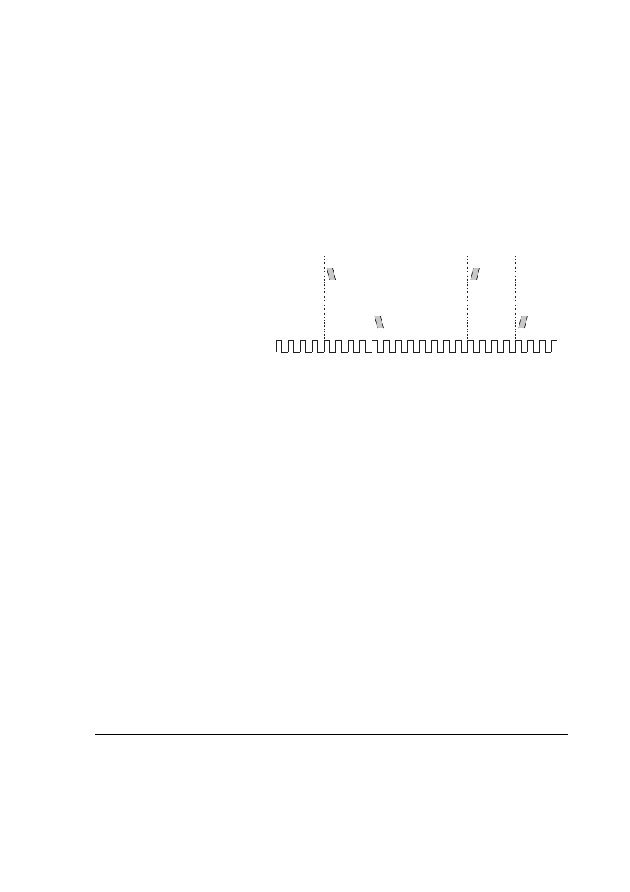
Figure 12-3 shows the sequence of events when a peripheral denies a system low-power
request.
Figure 12-3 Denial of a low-power request
In Figure 12-3, the peripheral denies a low-power request by holding
CACTIVE
HIGH
when it acknowledges the low-power request. After that point, the system clock
controller must complete the low-power request handshake by asserting
CSYSREQ
before it can initiate another request.
12.2.3
Exiting a low-power state
Either the system clock controller or the peripheral can request to exit the low-power
state and restore the clock. By definition, both
CACTIVE
and
CSYSREQ
are LOW
during the low power state, and driving either of these signals HIGH initiates the exit
sequence.
The system clock controller can initiate the exit from the low-power state by enabling
the clock and driving
CSYSREQ
HIGH. The peripheral can then perform a power-up
sequence in which it drives
CACTIVE
HIGH. Then it completes the exit by driving
CSYSACK
HIGH.
The peripheral can initiate the exit from a low-power state by driving
CACTIVE
HIGH.
The system clock controller must then immediately restore the clock. It must also drive
CSYSREQ
HIGH to continue the handshake sequence. The peripheral then completes
the sequence by driving
CSYSACK
HIGH while exiting the low-power state. The
peripheral can keep
CSYSACK
LOW for as many cycles as it requires to complete the
exit sequence.
CSYSREQ
T1
T2
T3
T4
CSYSACK
CACTIVE
CLK
Low-power Interface
12-6
Copyright © 2003, 2004 ARM Limited. All rights reserved.
ARM IHI 0022B
12.2.4
Clock control sequence summary
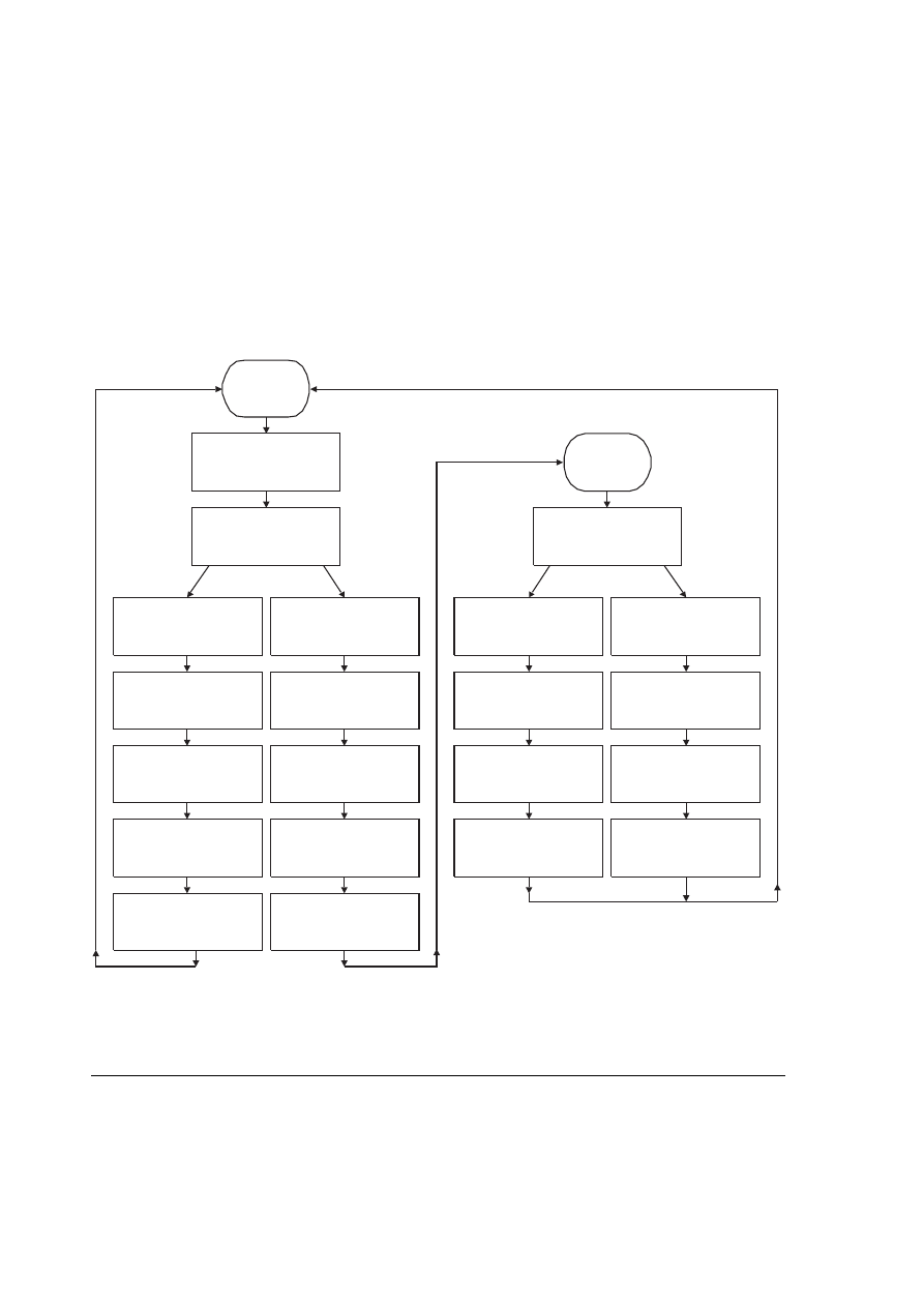
Figure 12-4 shows the typical flow for entering and exiting a low-power state.
Figure 12-4 Low-power clock control sequence
Normal
clocked
operation
Low -pow er
unclocked
operation
Peripheral or system
clock controller initiates
low -pow er exit
Peripheral
Peripheral drives
CACTIVE
HIGH
System clock controller
immediately enables
clocks
System clock
controller
System clock controller
drives
CSYSREQ
low to
request low -pow er entry
Peripheral denies or
accepts request
Peripheral keeps
CACTIVE
HIGH
Peripheral performs
pow er-dow n
Peripheral drives
CSYSACK
LOW to
acknow ledge request
Peripheral drives
CACTIVE
LOW
System clock controller
samples
CACTIVE
Peripheral drives
CSYSACK
LOW to
acknow ledge request
System clock controller
drives
CSYSREQ
HIGH
System clock controller
samples
CACTIVE
System clock controller
disables clocks
Deny
Accept
Peripheral drives
CSYSACK
HIGH to
complete handshake
Peripheral drives
CSYSACK
HIGH to
complete handshake
Peripheral drives
CSYSACK
HIGH to
complete handshake
System clock controller
drives
CSYSREQ
HIGH
Peripheral drives
CACTIVE
HIGH
System clock controller
immediately enables
clocks
System clock controller
drives
CSYSREQ
HIGH

Low-power Interface
ARM IHI 0022B
Copyright © 2003, 2004 ARM Limited. All rights reserved.
12-7
12.2.5
Combining peripherals in a low-power domain
The system clock controller can combine a number of different peripherals within the
same low-power clock domain. Then the clock domain can be treated in the same way
as a single peripheral if the following rules are observed:
•
The clock domain
CACTIVE
signal is the logical OR of all the
CACTIVE
signals within the clock domain. This means that the system clock controller can
disable the clocks only when all peripherals indicate that they can be disabled.
•
The system clock controller can use a single
CSYSREQ
signal that is routed to
all peripherals within the clock domain.
•
The clock domain
CSYSACK
signal is generated as follows:
—
the falling edge of
CSYSACK
occurs when the last falling edge from all of
the peripherals occurs
—
the rising edge of
CSYSACK
occurs when the last rising edge from all of
the peripherals occurs.

Low-power Interface
12-8
Copyright © 2003, 2004 ARM Limited. All rights reserved.
ARM IHI 0022B

ARM IHI 0022B
Copyright © 2003, 2004 ARM Limited. All rights reserved.
Index-1
Index
The items in this index are listed in alphabetical order with references to page numbers.
A
ACLK
definition 1-4
handshake 1-4, 3-2
Address ID tag
Addressing options 4-2
Allocate attribute 1-11
AMBA
architecture xiv
interface 1-2
Specification xvii
encoding 5-3
in exclusive accesses 6-5
ARESETn
in exclusive accesses 6-4, 6-5
out-of-order transactions 8-2
uniqueness 8-9
reset 11-2
timing example 1-7, 1-8
Atomic access encoding 6-2
AWADDR 2-3
encoding 5-3
in exclusive accesses 6-5
in exclusive accesses 6-5
out-of-order transactions 8-2
uniqueness 8-9