Материал: AMBA_v30_AXI_v10
Clock and Reset
11-2
Copyright © 2003, 2004 ARM Limited. All rights reserved.
ARM IHI 0022B
11.1
Clock and reset requirements
This section gives the requirements for implementing the
ACLK
and
ARESETn
signals.
11.1.1
Clock
Each AXI component uses a single clock signal,
ACLK
. All input signals are sampled
on the rising edge of
ACLK
. All output signal changes must occur after the rising edge
of
ACLK
.
There must be no combinatorial paths between input and output signals on both master
and slave interfaces.
11.1.2
Reset
The AXI protocol includes a single active LOW reset signal,
ARESETn
. The reset
signal can be asserted asynchronously, but deassertion must be synchronous after the
rising edge of
ACLK
.
During reset the following interface requirements apply:
•
a master interface must drive
ARVALID
,
AWVALID
, and
WVALID
LOW
•
a slave interface must drive
RVALID
and
BVALID
LOW.
All other signals can be driven to any value.
A master interface must begin driving
ARVALID
,
AWVALID
, or
WVALID
HIGH
only at a rising
ACLK
edge after
ARESETn
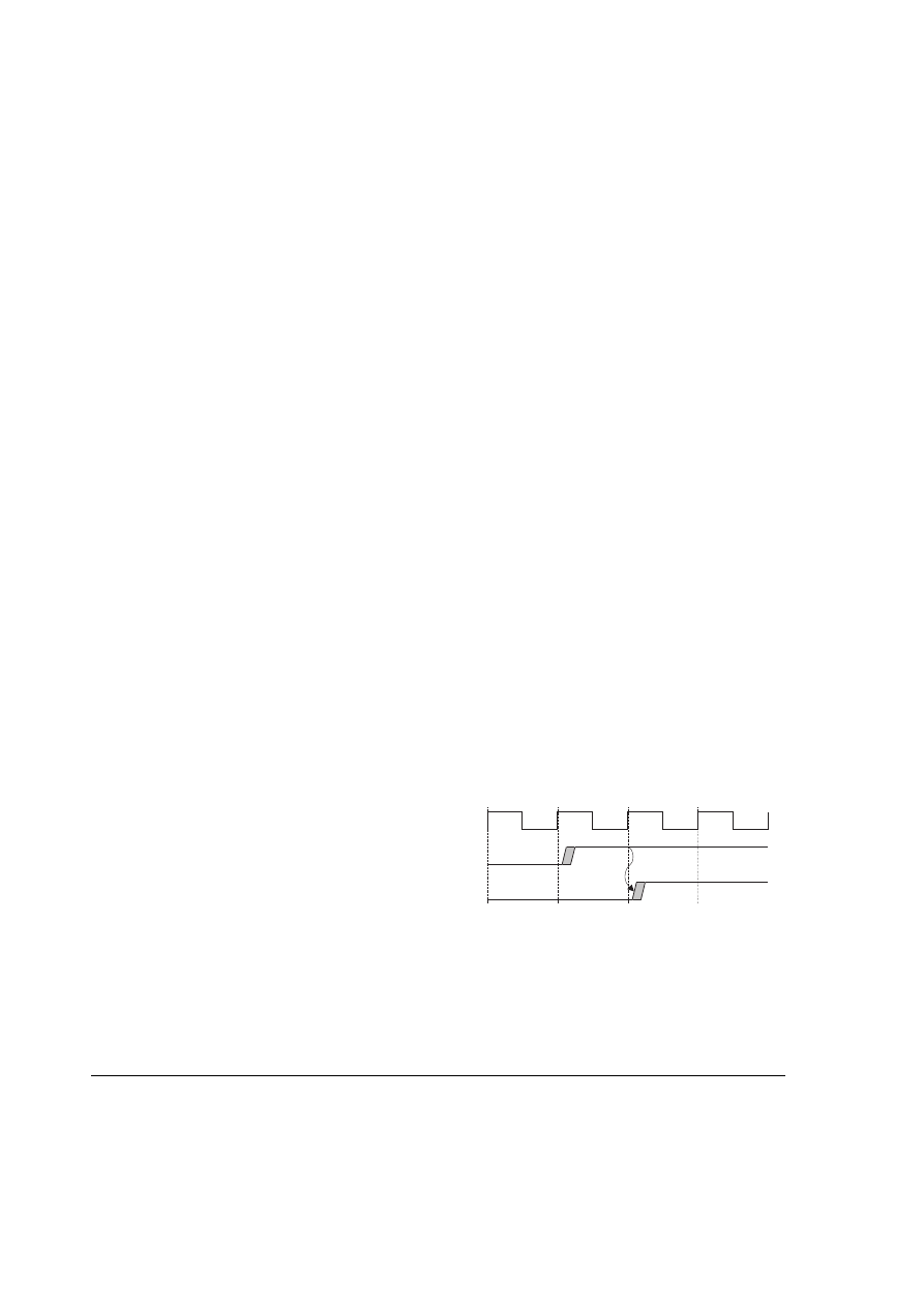
is HIGH. Figure 11-1 shows the first point
after reset that
ARVALID
,
AWVALID
, or
WVALID
, can be driven HIGH.
Figure 11-1 Exit from reset
ARESETn
VALID

ARM IHI 0022B
Copyright © 2003, 2004 ARM Limited. All rights reserved.
12-1
Chapter 12
Low-power Interface
This chapter describes the AXI protocol clock control interface during entry into and
exit from a low-power state. It contains the following sections:
•
•

Low-power Interface
12-2
Copyright © 2003, 2004 ARM Limited. All rights reserved.
ARM IHI 0022B
12.1
About the low-power interface
The low-power interface is an optional extension to the data transfer protocol that
targets two different classes of peripherals:
•
Peripherals that require a power-down sequence, and that can have their clocks
turned off only after they enter a low-power state. These peripherals require an
indication from a system clock controller to determine when to initiate the
power-down sequence.
•
Peripherals that have no power-down sequence, and that can independently
indicate when it is acceptable to turn off their clocks.
Low-power Interface
ARM IHI 0022B
Copyright © 2003, 2004 ARM Limited. All rights reserved.
12-3
12.2
Low-power clock control
The low-power clock control interface consists of the following signals:
•
a signal from the peripheral indicating when its clocks can be enabled or disabled
•
two handshake signals for the system clock controller to request exit or entry into
a low-power state.
The primary signal in the clock control interface is
CACTIVE
. The peripheral uses this
signal to indicate when it requires its clock to be enabled. The peripheral asserts
CACTIVE
to indicate that it requires the clock, and the system clock controller must
enable the clock immediately. The peripheral deasserts
CACTIVE
to indicate that it
does not require the clock. The system clock controller can then determine whether to
enable or disable the peripheral clock.
A peripheral that can have its clock enabled or disabled at any time can drive
CACTIVE
LOW permanently. A peripheral that must have its clock always enabled
must drive
CACTIVE
HIGH permanently.
This simple interface to the system clock controller is sufficient for some peripherals
with no power-down or power-up sequence.
For a more complex peripheral with a power-down or power-up sequence, entry into a
low-power state occurs only after a request from the system clock controller. The AXI
protocol provides a two-wire request/acknowledge handshake to support this request:
CSYSREQ
To request that the peripheral enter a low-power state, the system clock
controller drives the
CSYSREQ
signal LOW. During normal operation,
CSYSREQ
is HIGH.
CSYSACK
The peripheral uses the
CSYSACK
signal to acknowledge both the
low-power state request and the exit from the low-power state.
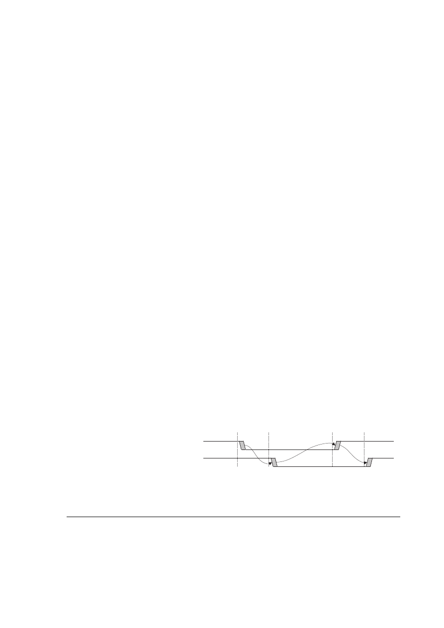
Figure 12-1 shows the relationship between
CSYSREQ
and
CSYSACK
.
Figure 12-1 CSYSREQ and CSYSACK handshake
CSYSREQ
CSYSACK
T1
T2
T3
T4
Low-power Interface
12-4
Copyright © 2003, 2004 ARM Limited. All rights reserved.
ARM IHI 0022B
At the start of the sequence in Figure 12-1 on page 12-3, both
CSYSREQ
and
CSYSACK
are HIGH for normal clocked operation. At time T1, the system clock
controller deasserts
CSYSREQ
, indicating a request to put the peripheral in a
low-power state. The peripheral acknowledges the request at time T2 by deasserting
CSYSACK
. At T3, the system clock controller asserts
CSYSREQ
to indicate the exit
from the low-power state, and the peripheral asserts
CSYSACK
at T4 to acknowledge
the exit.
This relationship between
CSYSREQ
and
CSYSACK
is a requirement of the AXI
protocol.
The peripheral can accept or deny the request for a low-power state from the system
clock controller. The level of the
CACTIVE
signal when the peripheral acknowledges
the request by deasserting
CSYSACK
indicates the acceptance or denial of the request.
12.2.1
Acceptance of low-power request
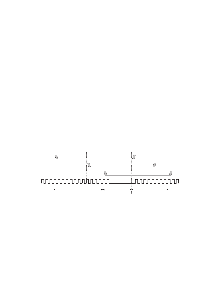
Figure 12-2 shows the sequence of events when a peripheral accepts a system
low-power request.
Figure 12-2 Acceptance of a low-power request
In Figure 12-2, the sequence begins at T1 when the system clock controller deasserts
CSYSREQ
to request that the peripheral enter a low power state. After the peripheral
recognizes the request, it can then perform its power-down function and deassert
CACTIVE
. The peripheral then deasserts
CSYSACK
at T3 to complete the entry into
the low-power state.
At T4, the system clock controller begins the low-power state exit sequence by asserting
CSYSREQ
. The peripheral then asserts
CACTIVE
at T5 and completes the exit
sequence at T6 by asserting
CSYSACK
.
Normal
operation
CSYSACK
T1
T2
T3
T4
T5
T6
Normal
operation
CACTIVE
CSYSREQ
Entry to
low power
Low
power
Exit from
low power
CLK