Материал: AMBA_v30_AXI_v10

ARM IHI 0022B
Copyright © 2003, 2004 ARM Limited. All rights reserved.
10-1
Chapter 10
Unaligned Transfers
This chapter describes how the AXI protocol handles unaligned transfers. It contains the
following sections:
•
•

Unaligned Transfers
10-2
Copyright © 2003, 2004 ARM Limited. All rights reserved.
ARM IHI 0022B
10.1
About unaligned transfers
The AXI protocol uses burst-based addressing, which means that each transaction
consists of a number of data transfers. Typically, each data transfer is aligned to the size
of the transfer. For example, a 32-bit wide transfer is usually aligned to four-byte
boundaries. However, there are times when it is desirable to begin a burst at an
unaligned address.
For any burst that is made up of data transfers wider than one byte, it is possible that the
first bytes that have to be accessed do not align with the natural data width boundary.
For example, a 32-bit (four-byte) data packet that starts at a byte address of
0x1002
is not
aligned to a 32-bit boundary.
The AXI protocol enables a master to use the low-order address lines to signal an
unaligned start address for a burst. The information on the low-order address lines must
be consistent with the information contained on the byte lane strobes.
Note
The AXI protocol does not require the slave to take special action based on any
alignment information from the master.
The master can also simply provide an aligned address and, in a write transaction, rely
on the byte lane strobes to provide the information about which byte lanes the data is
using.
Unaligned Transfers
ARM IHI 0022B
Copyright © 2003, 2004 ARM Limited. All rights reserved.
10-3
10.2
Examples
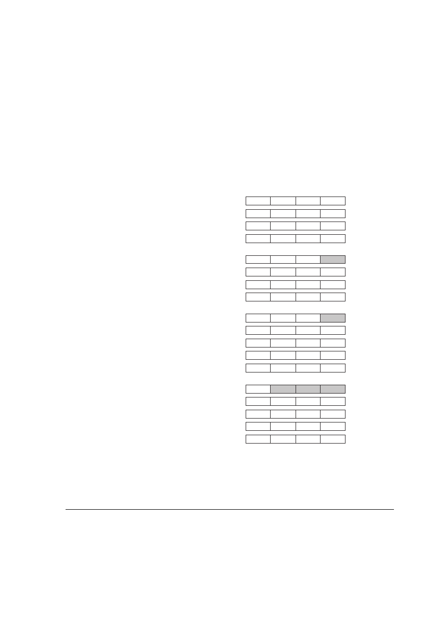
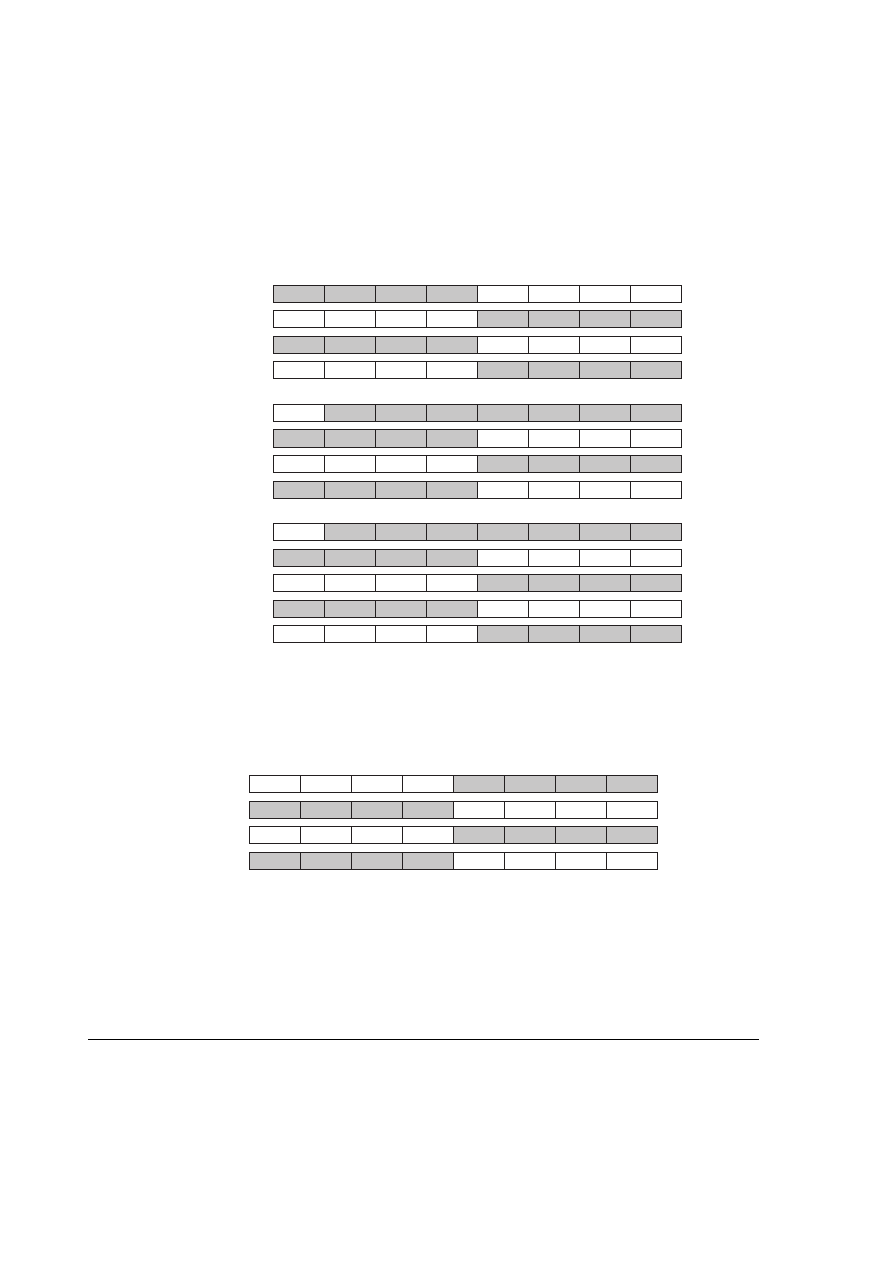
Figure 10-1, Figure 10-2 on page 10-4, and Figure 10-3 on page 10-4 show examples
of aligned and unaligned transfers on buses with different widths. Each row in the
figures represents a transfer. The shaded cells indicate bytes that are not transferred,
based on the address and control information.
Figure 10-1 Aligned and unaligned word transfers on a 32-bit bus
Figure 10-2 on page 10-4 shows three bursts of 32-bit transfers on a 64-bit bus.
0
0
6
5
4
Address:
0x00
Transfer size: 32 bits
Burst type: incrementing
Burst length: 4 transfers
3
2
1
0
7
6
5
4
B
A
9
8
F
E
D
C
3
2
1
7
6
5
4
B
A
9
8
F
E
D
C
Address:
0x01
Transfer size: 32 bits
Burst type: incrementing
Burst length: 4 transfers
3
2
1
7
6
5
4
B
A
9
8
F
E
D
C
Address:
0x01
Transfer size: 32 bits
Burst type: incrementing
Burst length: 5 transfers
13
12
11
10
7
B
A
9
8
F
E
D
C
13
12
11
10
17
16
15
14
Address:
0x07
Transfer size: 32 bits
Burst type: incrementing
Burst length: 5 transfers
1st transfer
2nd transfer
3rd transfer
4th transfer
1st transfer
2nd transfer
3rd transfer
4th transfer
1st transfer
2nd transfer
3rd transfer
4th transfer
5th transfer
1st transfer
2nd transfer
3rd transfer
4th transfer
5th transfer
0
7
15
8
16
23
24
31
Unaligned Transfers
10-4
Copyright © 2003, 2004 ARM Limited. All rights reserved.
ARM IHI 0022B
Figure 10-2 Aligned and unaligned word transfers on a 64-bit bus
Figure 10-3 shows a wrapping burst of 32-bit transfers on a 64-bit bus.
Figure 10-3 Aligned wrapping word transfers on a 64-bit bus
4
4
Address:
0x00
Transfer size: 32 bits
Burst type: incrementing
Burst length: 4 transfers
7
6
5
4
7
6
5
4
F
E
D
C
F
E
D
C
7
6
5
F
E
D
C
F
E
D
C
17
16
15
14
Address:
0x07
Transfer size: 32 bits
Burst type: incrementing
Burst length: 4 transfers
7
6
5
F
E
D
C
F
E
D
C
17
16
15
14
Address:
0x07
Transfer size: 32 bits
Burst type: incrementing
Burst length: 5 transfers
17
16
15
14
3
2
1
0
3
2
1
0
B
A
9
8
B
A
9
8
0
3
2
1
B
A
9
8
B
A
9
8
13
12
11
10
0
3
2
1
B
A
9
8
B
A
9
8
13
12
11
10
13
12
11
10
1st transfer
2nd transfer
3rd transfer
4th transfer
5th transfer
1st transfer
2nd transfer
3rd transfer
4th transfer
1st transfer
2nd transfer
3rd transfer
4th transfer
0
7
15
8
16
23
24
31
32
39
47
40
48
55
56
63
Address:
0x04
Transfer size: 32 bits
Burst type: wrapping
Burst length: 4 transfers
7
6
5
4
F
E
D
C
F
E
D
C
7
6
5
4
3
2
1
0
B
A
9
8
B
A
9
8
3
2
1
0
1st transfer
2nd transfer
3rd transfer
4th transfer
0
7
15
8
16
23
24
31
32
39
47
40
48
55
56
63

ARM IHI 0022B
Copyright © 2003, 2004 ARM Limited. All rights reserved.
11-1
Chapter 11
Clock and Reset
This chapter describes the timing of the AXI clock and reset signals. It contains the
following section:
•