Материал: AMBA_v30_AXI_v10

Data Buses
9-2
Copyright © 2003, 2004 ARM Limited. All rights reserved.
ARM IHI 0022B
9.1
About the data buses
The AXI protocol has two independent data buses, one for read data and one for write
data. Because these data buses have their own individual handshake signals, it is
possible for data transfers to occur on both buses at the same time.
Every transfer generated by a master must be the same width as or narrower than the
data bus for the transfer.
Data Buses
ARM IHI 0022B
Copyright © 2003, 2004 ARM Limited. All rights reserved.
9-3
9.2
Write strobes
The write strobe signals,
WSTRB
, enable sparse data transfer on the write data bus.
Each write strobe signal corresponds to one byte of the write data bus. When asserted,
a write strobe indicates that the corresponding byte lane of the data bus contains valid
information to be updated in memory.
There is one write strobe for each eight bits of the write data bus, so
WSTRB[n]
corresponds to
WDATA[(8
×
n) + 7: (8
×
n)]
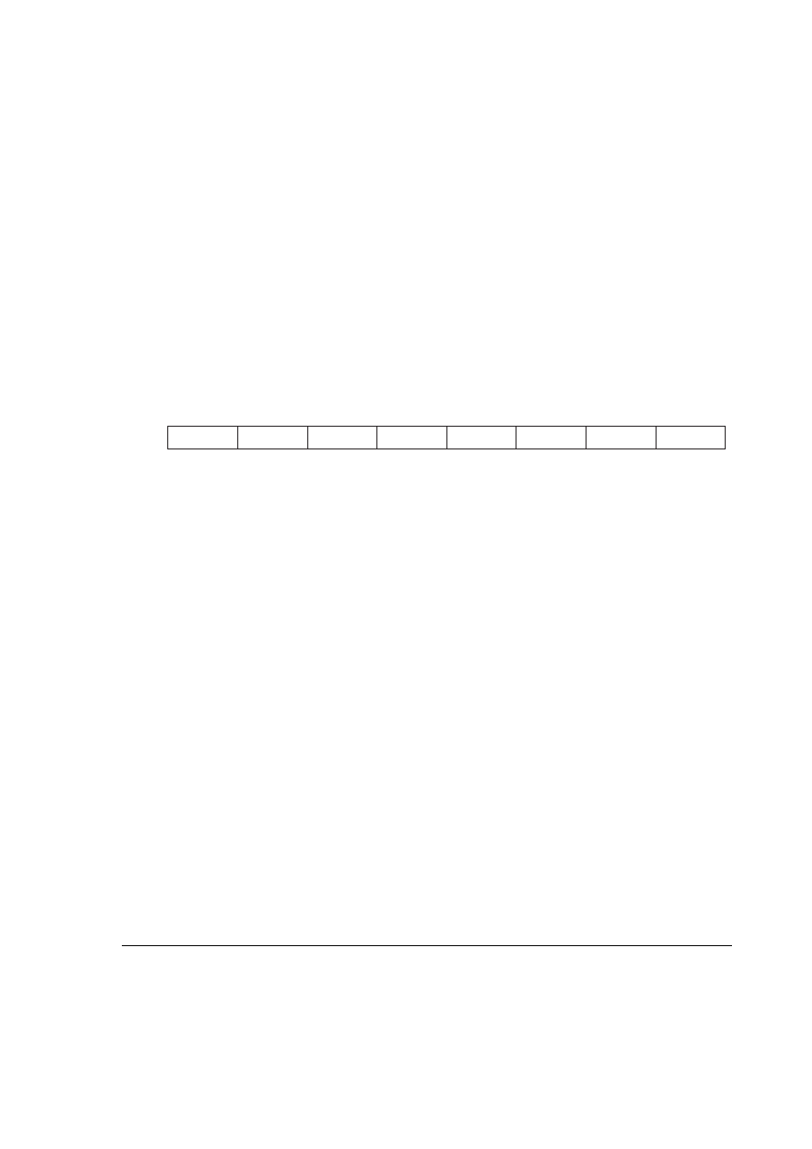
. Figure 9-1 shows this relationship on a
64-bit data bus.
Figure 9-1 Byte lane mapping
A master must ensure that the write strobes are asserted only for byte lanes that can
contain valid data as determined by the control information for the transaction.
7
6
5
3
4
2
1
0
63
56 55
48 47
40 39
32 31
24 23
16 15
8 7
0

Data Buses
9-4
Copyright © 2003, 2004 ARM Limited. All rights reserved.
ARM IHI 0022B
9.3
Narrow transfers
When a master generates a transfer that is narrower than its data bus, the address and
control information determine which byte lanes the transfer uses. In incrementing or
wrapping bursts, different byte lanes transfer the data on each beat of the burst. In a fixed
burst, the address remains constant, and the byte lanes that can be used also remain
constant.
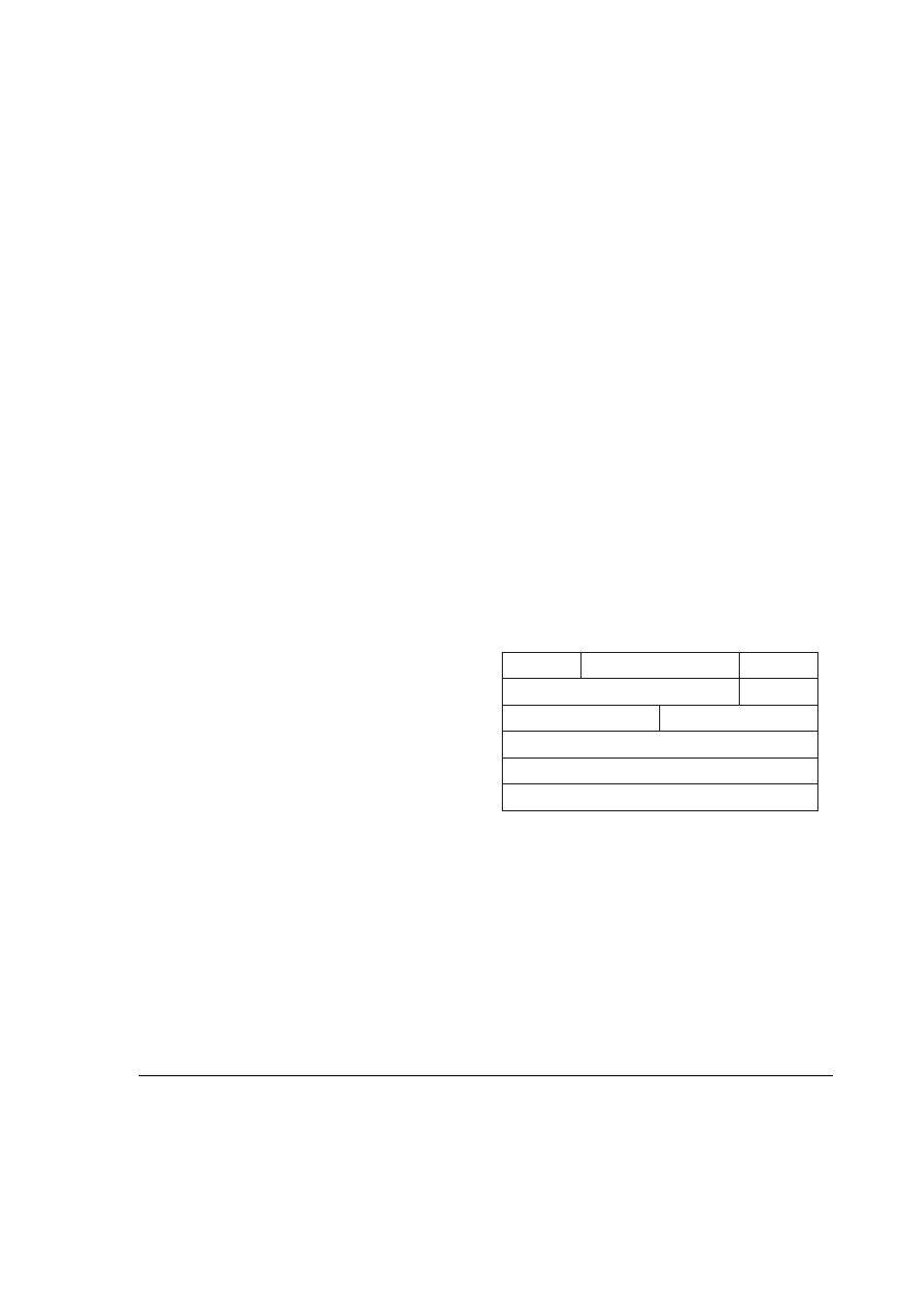
Figure 9-2 and Figure 9-3 give two examples of byte lanes use.
•
the burst has five transfers
•
the starting address is 0
•
each transfer is eight bits
•
the transfers are on a 32-bit bus.
Figure 9-2 Narrow transfer example with 8-bit transfers
•
the burst has three transfers
•
the starting address is 4
•
each transfer is 32 bits
•
the transfers are on a 64-bit bus.
Figure 9-3 Narrow transfer example with 32-bit transfers
DATA[7:0]
DATA[15:8]
DATA[23:16]
DATA[31:24]
DATA[7:0]
Byte lane used
1st transfer
2nd transfer
3rd transfer
4th transfer
5th transfer
DATA[63:32]
DATA[31:0]
DATA[63:32]
Byte lane used
1st transfer
2nd transfer
3rd transfer
Data Buses
ARM IHI 0022B
Copyright © 2003, 2004 ARM Limited. All rights reserved.
9-5
9.4
Byte invariance
To access mixed-endian data structures that reside in the same memory space, the AXI
protocol uses a byte-invariant endian scheme.
Byte-invariant endianness means that a byte transfer to a given address passes the eight
bits of data on the same data bus wires to the same address location.
Components that have only one transfer width must have their byte lanes connected to
the appropriate byte lanes of the data bus. Components that support multiple transfer
widths might require a more complex interface to convert an interface that is not
naturally byte-invariant.
Most little-endian components can connect directly to a byte-invariant interface.
Components that support only big-endian transfers require a conversion function for
byte-invariant operation.
Figure 9-4 is an example of a data structure requiring byte-invariant access. It is
possible that the header information, such as the source and destination identifiers, is in
little-endian format, but the payload is a big-endian byte stream.
Figure 9-4 Example mixed-endian data structure
Byte invariance ensures that little-endian access to parts of the header information does
not corrupt other big-endian data within the structure.
Packet
Source
Desti-
-nation
Checksum
Data items
Payload
Payload
Payload
Payload
31
0
7
23
24
8

Data Buses
9-6
Copyright © 2003, 2004 ARM Limited. All rights reserved.
ARM IHI 0022B