Материал: Packages_Diodes_Inc
Внимание! Если размещение файла нарушает Ваши авторские права, то обязательно сообщите нам

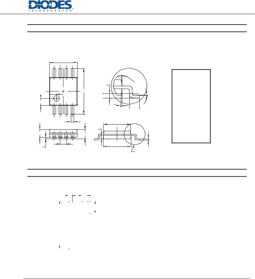
Package Outline Dimensions

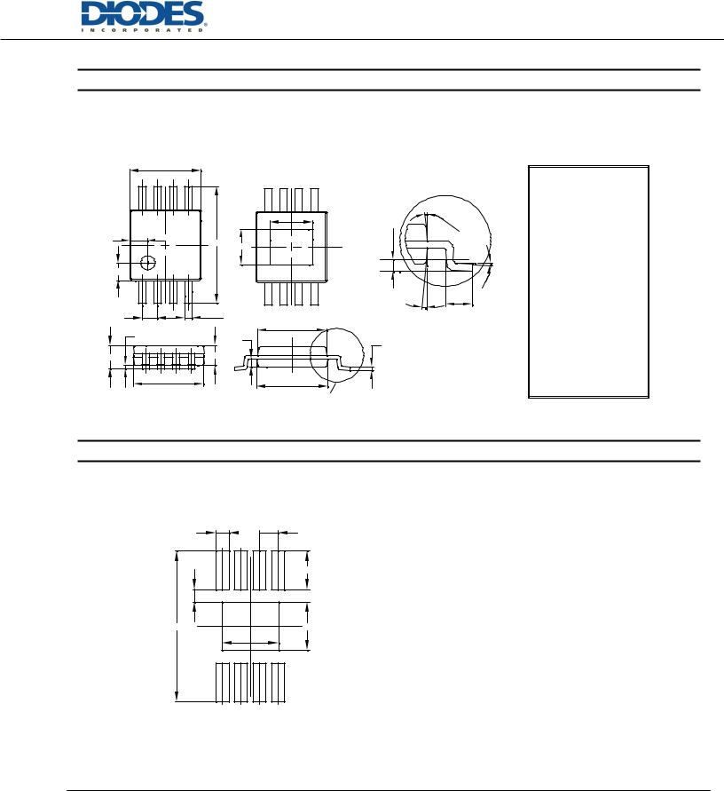
MSOP-8

D

x

y

1b

A2

e

A1

4


X


1


0


°

0.25


E

GaugePlane

Seating Plane

L a 4X10°

DetailC

E3


A3


A


E1

c


SeDetailC

MSOP-8

Dim

Min

Max

Typ

A

-

1.10

-

A1

0.05

0.15

0.10

A2

0.75

0.95

0.86

A3

0.29

0.49

0.39

b

0.22

0.38

0.30

c

0.08

0.23

0.15

D

2.90

3.10

3.00

E

4.70

5.10

4.90

E1

2.90

3.10

3.00

E3

2.85

3.05

2.95

e

-

-

0.65

L

0.40

0.80

0.60

a

x

-

-

0.750

y

-

-

0.750

All Dimensions in mm

Suggested Pad Layout

MSOP-8


X


C


Y


Dimensions

Value


(in mm)


C

0.650


X

0.450

Y1


Y

1.350


Y1

5.300


ALL DIMENSIONS ARE NOMINAL VALUES SHOWN IN MILLIMETERS

Note: The suggested land pattern dimensions have been provided for reference only, as actual pad layouts may vary depending on application. These numbers may be modified based on user equipment capability or fabrication criteria. A more robust pattern may be desired for wave soldering and is calculated by adding 0.2 mm to the ‘Z’ dimension. For further information, please reference document IPC-7351A, Naming Convention for Standard SMT Land Patterns, and for International grid details, please see document IEC, Publication 97.

Rev. 76

111 of 263

Package Outline Dimensions


www.diodes.com

Suggested Pad Layout


© Diodes Incorporated

Package Outline Dimensions


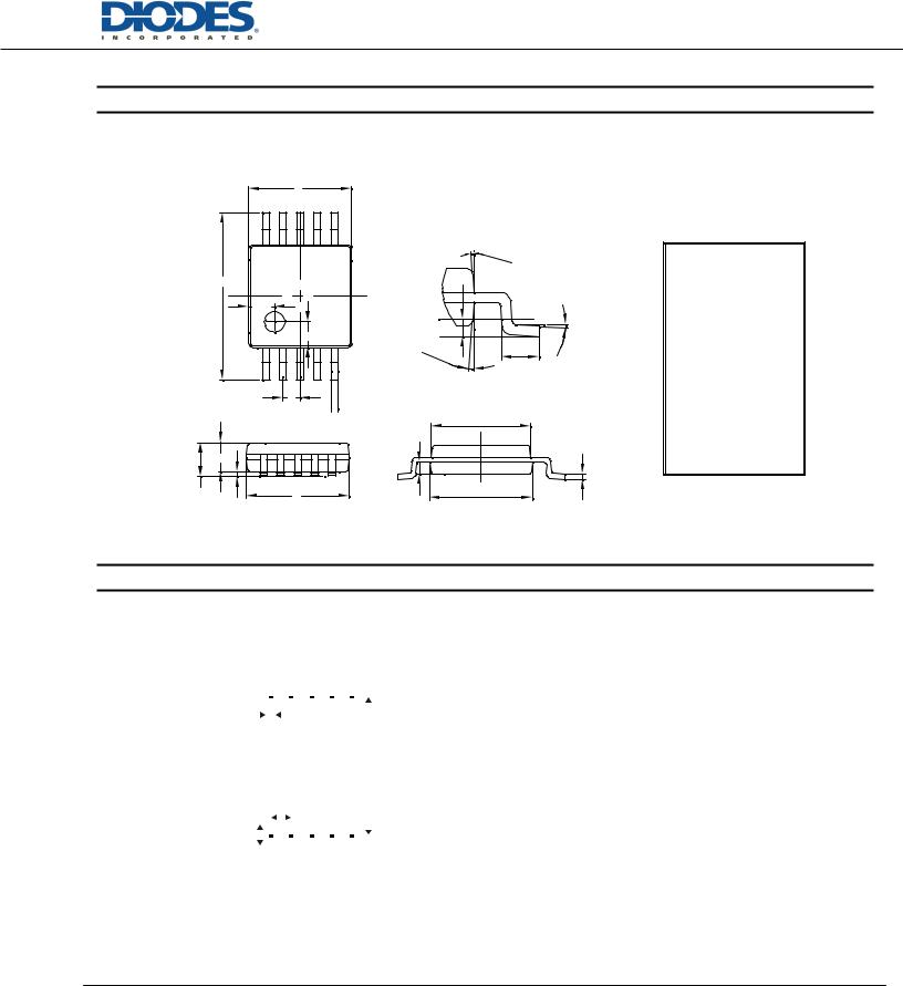
MSOP-8EP


D


D1


X


E


0.25


4

1


0


°


x


E2


GaugePlane


y


Seating Plane


a


4


X


L


1


1


8Xb


e


DetailC


E3


A1

A3


c


A

A2


D


E1


SeDetailC


MSOP-8EP

Dim

Min

Max

Typ

A

-

1.10

-

A1

0.05

0.15

0.10

A2

0.75

0.95

0.86

A3

0.29

0.49

0.39

b

0.22

0.38

0.30

c

0.08

0.23

0.15

D

2.90

3.10

3.00

D1

1.60

2.00

1.80

E

4.70

5.10

4.90

E1

2.90

3.10

3.00

E2

1.30

1.70

1.50

E3

2.85

3.05

2.95

e

-

-

0.65

L

0.40

0.80

0.60

a

x

-

-

0.750

y

-

-

0.750

All Dimensions in mm

Suggested Pad Layout

X C

G

Y2

X1

MSOP8-EP

Y

Y1

Dimensions

Value

(in mm)


C

0.650

G

0.450

X

0.450

X1

2.000

Y

1.350

Y1

1.700

Y2

5.300

ALL DIMENSIONS ARE NOMINAL VALUES SHOWN IN MILLIMETERS

Note: The suggested land pattern dimensions have been provided for reference only, as actual pad layouts may vary depending on application. These numbers may be modified based on user equipment capability or fabrication criteria. A more robust pattern may be desired for wave soldering and is calculated by adding 0.2 mm to the ‘Z’ dimension. For further information, please reference document IPC-7351A, Naming Convention for Standard SMT Land Patterns, and for International grid details, please see document IEC, Publication 97.

Rev. 76

112 of 263

Package Outline Dimensions


www.diodes.com

Suggested Pad Layout


© Diodes Incorporated

Package Outline Dimensions

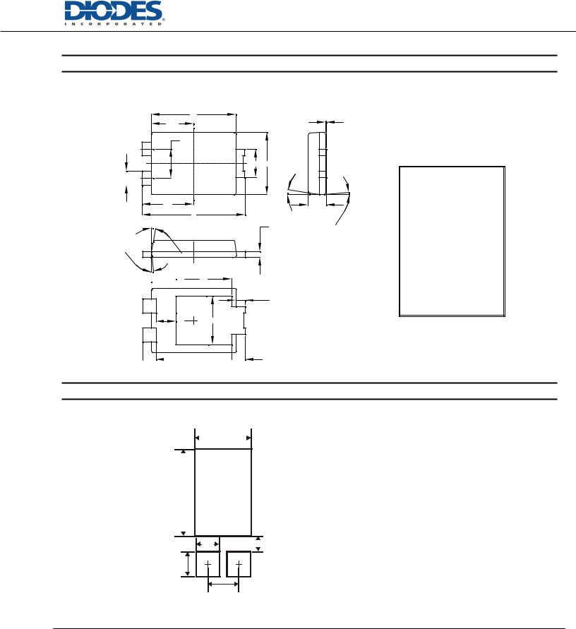
MSOP-10

D

4

X10°


E


0.25


X

Gauge Plane


Y

Seating Plane


4X

10°

L

a


1


e


b (10X)


E3


A2


A

D

A3

E1


A1

c


MSOP-10

Dim

Min

Max

Typ

a

A

-

1.10

-

A1

0.05

0.15

0.10

A

0.75

0.95

0.86

b

0.17

0.27

0.20

c

0.08

0.23

0.15

D

2.95

3.05

3.00

e

-

-

0.50

E

4.80

5.00

4.90

E1

2.95

3.05

3.00

L

0.40

0.80

0.60


All Dimensions in mm

Suggested Pad Layout

MSOP-10


X


Dimensions

Value


(in mm)


C1

X

0.30


Y

1.4


C1

4.4


C2


C2

0.50


Y


ALL DIMENSIONS ARE NOMINAL VALUES SHOWN IN MILLIMETERS

Note: The suggested land pattern dimensions have been provided for reference only, as actual pad layouts may vary depending on application. These numbers may be modified based on user equipment capability or fabrication criteria. A more robust pattern may be desired for wave soldering and is calculated by adding 0.2 mm to the ‘Z’ dimension. For further information, please reference document IPC-7351A, Naming Convention for Standard SMT Land Patterns, and for International grid details, please see document IEC, Publication 97.

Rev. 76

113 of 263

Package Outline Dimensions


www.diodes.com

Suggested Pad Layout


© Diodes Incorporated

Package Outline Dimensions


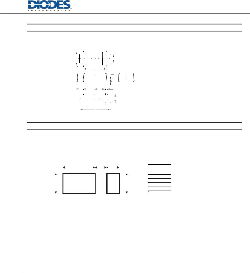
POWERDI®5


E1


A1

E1/2


e


°


1


±


°


b2D

0


1


2Xb1


E/2


A


5


°


±

E


1


A2


°


1


0


°


±

5

1

°

°


±


1


°


L1 E2

L1

W

D2

POWERDI®5

Dim

Min

Max

Typ

A

1.05

1.15

1.10

A2

0.33

0.43

0.381

b1

0.80

0.99

0.89

b2

1.70

1.88

1.78

D

3.90

4.05

3.966

D2

-

-

3.054

E

6.40

6.60

6.504

e

-

-

1.84

E1

5.30

5.45

5.37

E2

-

-

3.549

L

0.75

0.95

0.85

L1

0.50

0.65

0.57

W

1.10

1.41

1.255

All Dimensions in mm

L L

Suggested Pad Layout

POWERDI®5


X


Dimensions

Value (in mm)


C

1.840


G

0.852

Y


X

3.360


X1

1.390


Y

4.860


Y1

1.400


X1


G


(2x)


Y1

(2x)

C

ALL DIMENSIONS ARE NOMINAL VALUES SHOWN IN MILLIMETERS

Note: The suggested land pattern dimensions have been provided for reference only, as actual pad layouts may vary depending on application. These numbers may be modified based on user equipment capability or fabrication criteria. A more robust pattern may be desired for wave soldering and is calculated by adding 0.2 mm to the ‘Z’ dimension. For further information, please reference document IPC-7351A, Naming Convention for Standard SMT Land Patterns, and for International grid details, please see document IEC, Publication 97.

Rev. 76

114 of 263

Package Outline Dimensions


www.diodes.com

Suggested Pad Layout


© Diodes Incorporated

Package Outline Dimensions


POWERDI®123


POWERDI®123


C


E


Dim


Min

Max

Typ


A


3.50

3.90

3.70


B


2.60

3.00

2.80


B


C


1.63

1.93

1.78


H


D


0.93

1.00

0.98

D


E


0.85

1.25

1.00


H


0.15

0.25

0.20


L L1


L


0.40

0.50

0.45


L3


L1


1.25

1.40

1.35


L2


1.025

1.125

1.10


L2


L3


0.125

0.275

0.20


All Dimensions in mm


A


Suggested Pad Layout

POWERDI®123


X1


G


X2


Dimensions

POWERDI®123

POWERDI®323


G

1.0

0.5


X1


2.2

2.0


X2


0.9

0.8

Y2


Y1


Y1


1.4

0.8


Y2


1.4

1.1


ALL DIMENSIONS ARE NOMINAL VALUES SHOWN IN MILLIMETERS

Note: The suggested land pattern dimensions have been provided for reference only, as actual pad layouts may vary depending on application. These numbers may be modified based on user equipment capability or fabrication criteria. A more robust pattern may be desired for wave soldering and is calculated by adding 0.2 mm to the ‘Z’ dimension. For further information, please reference document IPC-7351A, Naming Convention for Standard SMT Land Patterns, and for International grid details, please see document IEC, Publication 97.

Rev. 76

115 of 263

Package Outline Dimensions


www.diodes.com

Suggested Pad Layout


© Diodes Incorporated

Источник: https://studfile.net/preview/16440213/