Материал: Packages_Diodes_Inc
Внимание! Если размещение файла нарушает Ваши авторские права, то обязательно сообщите нам

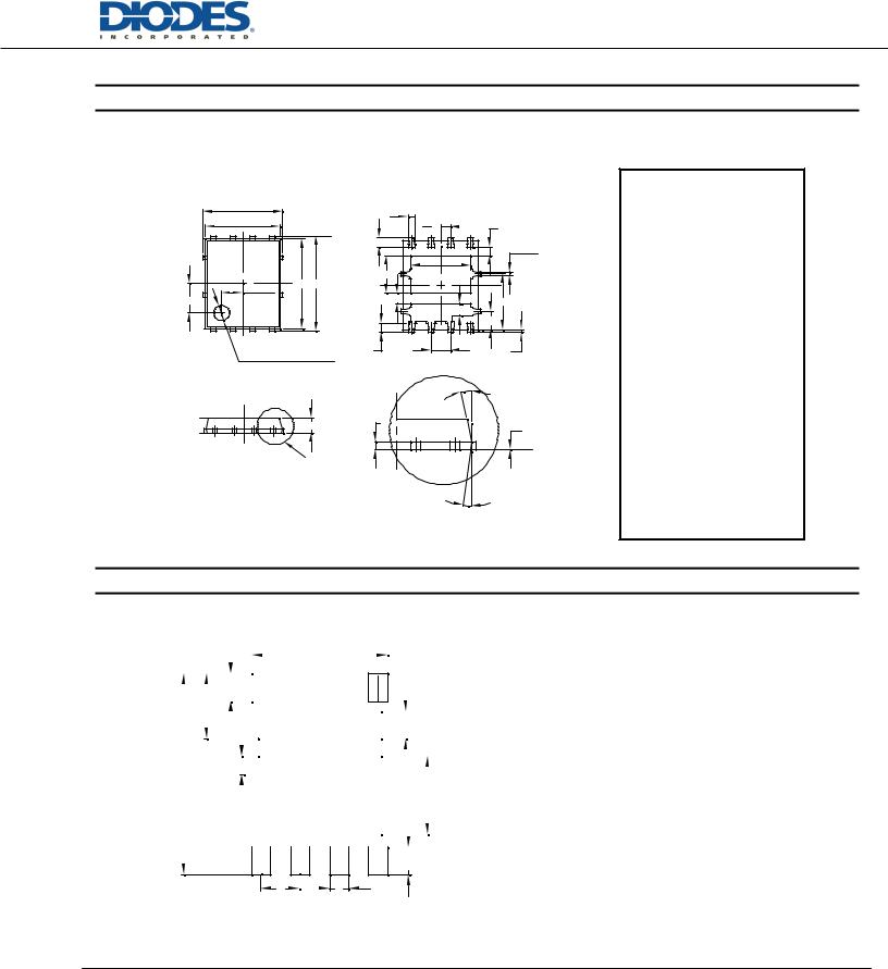
Package Outline Dimensions


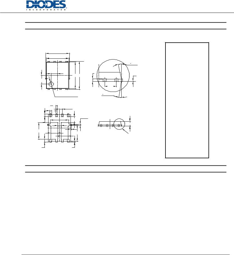
POWERDI®5060-8 (Type B)


D


b8X


D1


e/2


K


L


b24X


D2


E1E

E2


1.40


K1


1.90


M


E3

M1


Ø1.0Depth07±..03

G

e


L1


θ (4 )


X


A

c


A1


DETAIL A


θ1 X(4 )

POWERDI®5060-8

TYPE B

Dim

Min

Max

Typ

A

0.90

1.10

1.00

A1

0.00

0.05

––

b

0.33

0.51

0.41

b2

0.20

0.40

0.273

c

0.230

0.330

0.273

D


5.15 BSC


D1

4.70

5.10

4.90

D2

3.50

4.40

3.90

E


6.15 BSC


E1

5.60

6.00

5.80

E2

2.25

2.65

2.45

E3

0.595

0.995

0.795

e


1.27 BSC


G

0.51

0.71

0.61

K

0.51

––

––

K1

0.51

––

––

L

0.51

0.71

0.61

L1

0.05

0.20

0.175

M

3.235

4.035

3.635

M1

1.00

1.40

1.21

θ1

10°

12°

11°

θ2

All Dimensions in mm

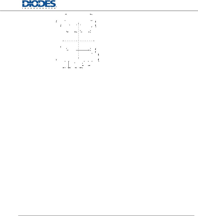
Suggested Pad Layout

POWERDI®5060-8 (Type B)


X1


Y1


Dimensions

Value (in mm)


Y3


C

1.270


Y2


X

0.610


X1

4.420


Y

0.910

Y6


Y1

0.910


Y2

0.895


Y4


Y5


Y3

2.130


Y4

0.585


Y5

2.550


Y6

6.550


Y5x


C X

ALL DIMENSIONS ARE NOMINAL VALUES SHOWN IN MILLIMETERS

Note: The suggested land pattern dimensions have been provided for reference only, as actual pad layouts may vary depending on application. These numbers may be modified based on user equipment capability or fabrication criteria. A more robust pattern may be desired for wave soldering and is calculated by adding 0.2 mm to the ‘Z’ dimension. For further information, please reference document IPC-7351A, Naming Convention for Standard SMT Land Patterns, and for International grid details, please see document IEC, Publication 97.

Rev. 76

121 of 263

Package Outline Dimensions


www.diodes.com

Suggested Pad Layout


© Diodes Incorporated

Package Outline Dimensions


PowerDI5060-8 (Type C)


D


D1


04x


x


c

A1


E1E


y


Seating Plane


e


1


Ø1.0Depth07±..03


014x


DETAIL A


b18x

e/2


b8x


1


D3


b22x


L


k


k1


A

E2


D2

L4


M


DETAIL A


D2


La


L1


PowerDI5060-8 (Type C)

Dim

Min


Max


Typ

A

0.90


1.10


1.00

A1

0


0.05


0.02

b

0.33


0.51


0.41

b1

0.300


0.366


0.333

b2

0.20


0.35


0.25

c

0.23


0.33


0.277

D


5.15 BSC


D1

4.85


4.95


4.90

D2

1.40


1.60


1.50

D3

-


-


3.98

E


6.15 BSC


E1

5.75


5.85


5.80

E2

3.56


3.76


3.66

e


1.27BSC


k

-


-


1.27

k1

0.56


-


-

L

0.51


0.71


0.61

La

0.51


0.71


0.61

L1

0.05


0.20


0.175

L4

-


-


0.125

M

3.50


3.71


3.605

x

-


-


1.400

y

-


-


1.900

θ

10°


12°


11°

θ1


All Dimensions in mm

Suggested Pad Layout

PowerDI5060-8 (Type C)

ALL DIMENSIONS ARE NOMINAL VALUES SHOWN IN MILLIMETERS

Note: The suggested land pattern dimensions have been provided for reference only, as actual pad layouts may vary depending on application. These numbers may be modified based on user equipment capability or fabrication criteria. A more robust pattern may be desired for wave soldering and is calculated by adding 0.2 mm to the ‘Z’ dimension. For further information, please reference document IPC-7351A, Naming Convention for Standard SMT Land Patterns, and for International grid details, please see document IEC, Publication 97.

Rev. 76

122 of 263

Package Outline Dimensions


www.diodes.com

Suggested Pad Layout


© Diodes Incorporated


X4


8


Dimensions

Value


(in mm)


C

1.270


X3


Y1

G

0.660


X2


G1

0.820


Y2


X

0.610


X1

3.910

Y3


G1

X2

1.650


X3

1.650


X1


X4

4.420


Y

1.270


Y4x

Y1

1.020


Y2

3.810


Y3

6.610


1


X


C


G


ALL DIMENSIONS ARE NOMINAL VALUES SHOWN IN MILLIMETERS

Note: The suggested land pattern dimensions have been provided for reference only, as actual pad layouts may vary depending on application. These numbers may be modified based on user equipment capability or fabrication criteria. A more robust pattern may be desired for wave soldering and is calculated by adding 0.2 mm to the ‘Z’ dimension. For further information, please reference document IPC-7351A, Naming Convention for Standard SMT Land Patterns, and for International grid details, please see document IEC, Publication 97.

Rev. 76

123 of 263

Package Outline Dimensions


www.diodes.com

Suggested Pad Layout


© Diodes Incorporated

Package Outline Dimensions

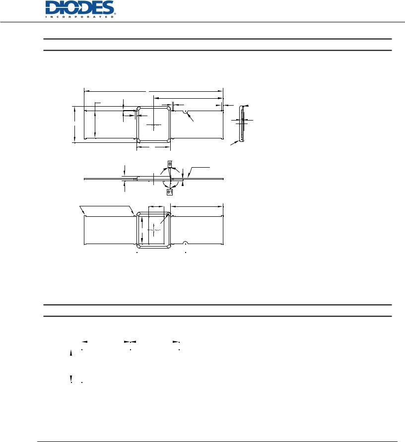
POWERDI®5SP


E

E/2


b 2x

J 4x

K 4x


M 4x

R


D

N 8x

3


E1


TOP VIEW


?

Cutting Burr Side


A


8x cut faces are not tin plated


H1


E2

' ?1


L 2x


R

D2

W L1

BOTTOM VIEW


POWERDI®5SP


R1

Dim

Min

Max

Typ

A

0.75


c

b

4.30

4.50

4.40

c

0.155

0.195


D

5.70

5.90

5.80


D2

4.40

R2

E

23.6

24.0

23.8

E1

5.70

5.90

5.80


E2

2.74


H1

0.19

0.21

0.20


J

0.20


K

0.30


L

9.00


L1

2.50


M

0.30


N

0

0.20


R

0.40


R1

0.15


R2

0.25


R3

0.40


W

1.66

2.06


θ

12º


θ1


All

Dimensions in mm

Suggested Pad Layout


X


G


Dimensions

Value


(in mm)


G

8.101

Y


X

8.100


Y

5.100

ALL DIMENSIONS ARE NOMINAL VALUES SHOWN IN MILLIMETERS

Note: The suggested land pattern dimensions have been provided for reference only, as actual pad layouts may vary depending on application. These numbers may be modified based on user equipment capability or fabrication criteria. A more robust pattern may be desired for wave soldering and is calculated by adding 0.2 mm to the ‘Z’ dimension. For further information, please reference document IPC-7351A, Naming Convention for Standard SMT Land Patterns, and for International grid details, please see document IEC, Publication 97.

Rev. 76

124 of 263

Package Outline Dimensions


www.diodes.com

Suggested Pad Layout


© Diodes Incorporated

Package Outline Dimensions

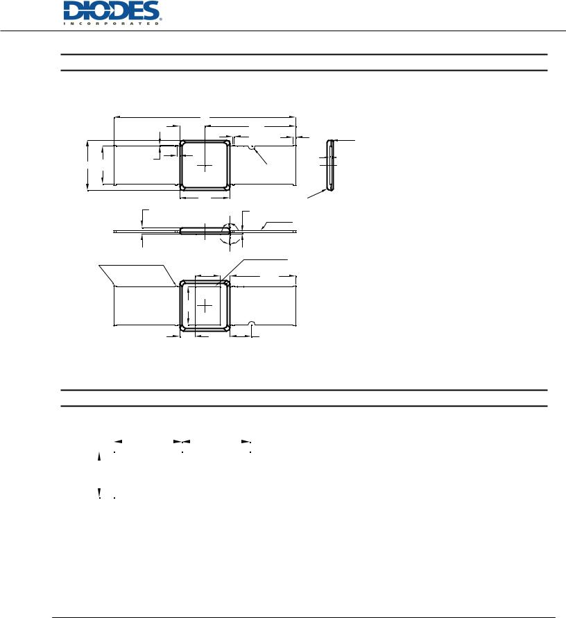
POWERDI®5SP (Type B)


E

E/2


E1/2

K 4x


J 4x


N 8x

M 4x

R


D

b 2x


3


2


E1


R


A

TOP VIEW

H1


ø

Cutting Burr Side


8x cut faces are not

ø1

V Groove Inner Line


tin plated

E2


L 2x


R

D2

W

L1

BOTTOM VIEW


POWERDI®5SP


R1


Type B


Dim

Min

Max

Typ


c


A

0.75


b

4.30

4.50

4.40


c

0.155

0.191


D

5.70

5.90

5.80


D2

4.40


E

20.8

21.2

21.0


E1

5.70

5.90

5.80


E2

2.90


H1

0.19

0.21

0.20


J

0.20


K

0.30


L

7.60


L1

2.50


M

0.30


N

0

0.20


R

0.40


R1

0.15


R2

0.25


R3

0.40


W

1.63

1.97

1.80


Ø

12º


Ø1


All

Dimensions in mm

Suggested Pad Layout


X


G


Dimensions

Value


(in mm)


G

8.101

Y


X

8.100


Y

5.100

ALL DIMENSIONS ARE NOMINAL VALUES SHOWN IN MILLIMETERS

Note: The suggested land pattern dimensions have been provided for reference only, as actual pad layouts may vary depending on application. These numbers may be modified based on user equipment capability or fabrication criteria. A more robust pattern may be desired for wave soldering and is calculated by adding 0.2 mm to the ‘Z’ dimension. For further information, please reference document IPC-7351A, Naming Convention for Standard SMT Land Patterns, and for International grid details, please see document IEC, Publication 97.

Rev. 76

125 of 263

Package Outline Dimensions


www.diodes.com

Suggested Pad Layout


© Diodes Incorporated

Источник: https://studfile.net/preview/16440213/