Материал: AMBA_v30_AXI_v10
Introduction
ARM IHI 0022B
Copyright © 2003, 2004 ARM Limited. All rights reserved.
1-3
1.2
Architecture
The AXI protocol is burst-based. Every transaction has address and control information
on the address channel that describes the nature of the data to be transferred. The data
is transferred between master and slave using a write data channel to the slave or a read
data channel to the master. In write transactions, in which all the data flows from the
master to the slave, the AXI protocol has an additional write response channel to allow
the slave to signal to the master the completion of the write transaction.
The AXI protocol enables:
•
address information to be issued ahead of the actual data transfer
•
support for multiple outstanding transactions
•
support for out-of-order completion of transactions.
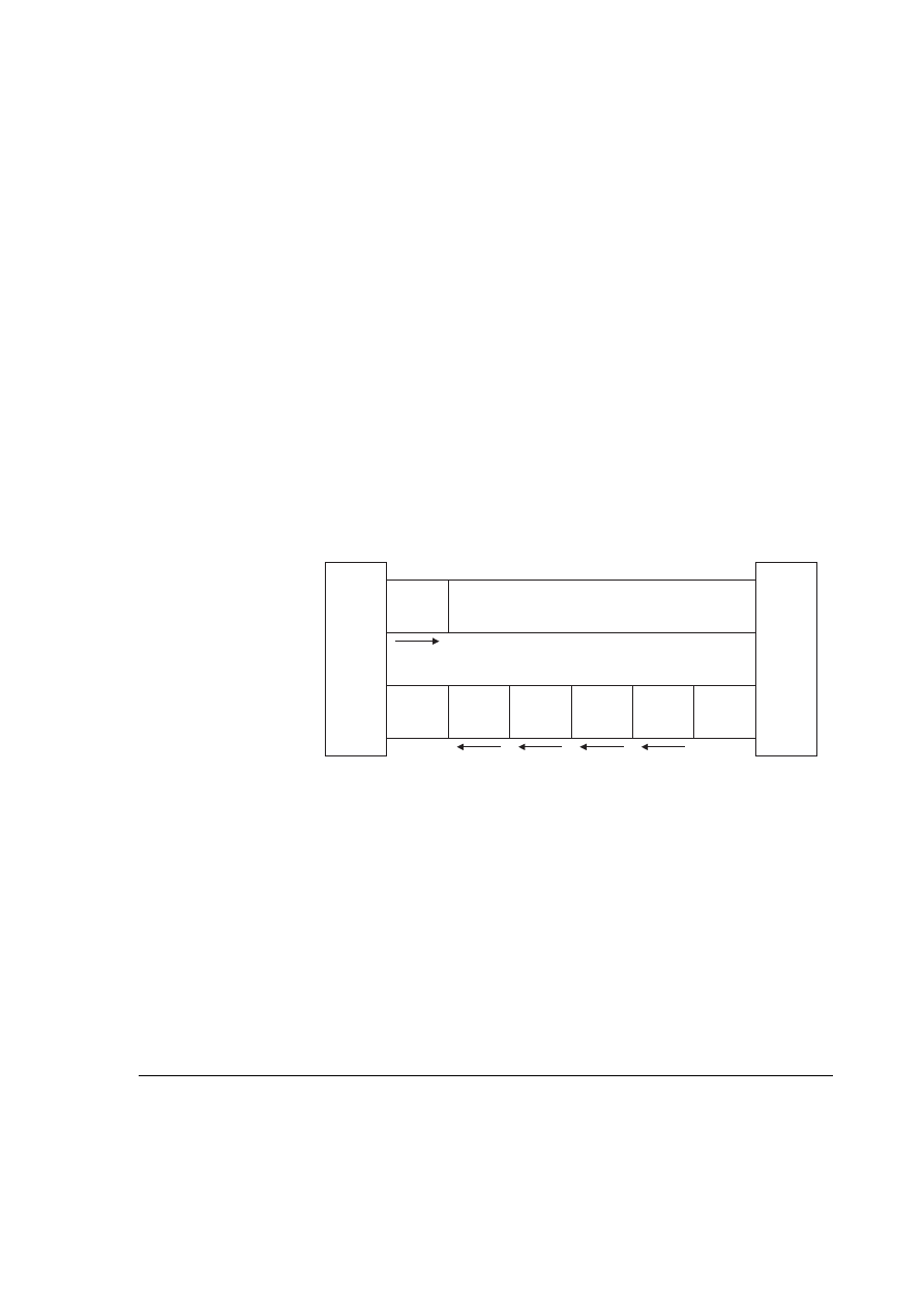
Figure 1-1 shows how a read transaction uses the read address and read data channels.
Figure 1-1 Channel architecture of reads
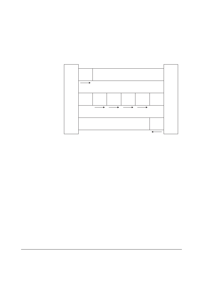
Figure 1-2 on page 1-4 shows how a write transaction uses the write address, write data,
and write response channels.
Master
interface
Slave
interface
Address
and
control
Read address channel
Read
data
Read
data
Read
data
Read
data
Read data channel
Introduction
1-4
Copyright © 2003, 2004 ARM Limited. All rights reserved.
ARM IHI 0022B
Figure 1-2 Channel architecture of writes
1.2.1
Channel definition
Each of the five independent channels consists of a set of information signals and uses
a two-way
VALID
and
READY
handshake mechanism.
The information source uses the
VALID
signal to show when valid data or control
information is available on the channel. The destination uses the
READY
signal to
show when it can accept the data. Both the read data channel and the write data channel
also include a
LAST
signal to indicate when the transfer of the final data item within a
transaction takes place.
Read and write address channels
Read and write transactions each have their own address channel. The appropriate
address channel carries all of the required address and control information for a
transaction. The AXI protocol supports the following mechanisms:
•
variable-length bursts, from 1 to 16 data transfers per burst
•
bursts with a transfer size of 8-1024 bits
•
wrapping, incrementing, and non-incrementing bursts
•
atomic operations, using exclusive or locked accesses
•
system-level caching and buffering control
Master
interface
Slave
interface
Address
and
control
Write address channel
Write
data
Write data channel
Write
data
Write
data
Write
data
Write
response
Write response channel

Introduction
ARM IHI 0022B
Copyright © 2003, 2004 ARM Limited. All rights reserved.
1-5
•
secure and privileged access.
Read data channel
The read data channel conveys both the read data and any read response information
from the slave back to the master. The read data channel includes:
•
the data bus, which can be 8, 16, 32, 64, 128, 256, 512, or 1024 bits wide
•
a read response indicating the completion status of the read transaction.
Write data channel
The write data channel conveys the write data from the master to the slave and includes:
•
the data bus, which can be 8, 16, 32, 64, 128, 256, 512, or 1024 bits wide
•
one byte lane strobe for every eight data bits, indicating which bytes of the data
bus are valid.
Write data channel information is always treated as buffered, so that the master can
perform write transactions without slave acknowledgement of previous write
transactions.
Write response channel
The write response channel provides a way for the slave to respond to write transactions.
All write transactions use completion signaling.
The completion signal occurs once for each burst, not for each individual data transfer
within the burst.
1.2.2
Interface and interconnect
A typical system consists of a number of master and slave devices connected together
through some form of interconnect, as shown in Figure 1-3.
Figure 1-3 Interface and interconnect
Interconnect
Slave 1
Slave 2
Slave 3
Slave 4
Master 1
Master 2
Master 3
Interface
Interface

Introduction
1-6
Copyright © 2003, 2004 ARM Limited. All rights reserved.
ARM IHI 0022B
The AXI protocol provides a single interface definition for describing interfaces:
•
between a master and the interconnect
•
between a slave and the interconnect
•
between a master and a slave.
The interface definition enables a variety of different interconnect implementations.
The interconnect between devices is equivalent to another device with symmetrical
master and slave ports to which real master and slave devices can be connected.
Most systems use one of three interconnect approaches:
•
shared address and data buses
•
shared address buses and multiple data buses
•
multilayer, with multiple address and data buses.
In most systems, the address channel bandwidth requirement is significantly less than
the data channel bandwidth requirement. Such systems can achieve a good balance
between system performance and interconnect complexity by using a shared address
bus with multiple data buses to enable parallel data transfers.
1.2.3
Register slices
Each AXI channel transfers information in only one direction, and there is no
requirement for a fixed relationship between the various channels. This is important
because it enables the insertion of a register slice in any channel, at the cost of an
additional cycle of latency. This makes possible a trade-off between cycles of latency
and maximum frequency of operation.
It is also possible to use register slices at almost any point within a given interconnect.
It can be advantageous to use a direct, fast connection between a processor and
high-performance memory, but to use simple register slices to isolate a longer path to
less performance-critical peripherals.
Introduction
ARM IHI 0022B
Copyright © 2003, 2004 ARM Limited. All rights reserved.
1-7
1.3
Basic transactions
This section gives examples of basic AXI protocol transactions. Each example shows
the
VALID
and
READY
handshake mechanism. Transfer of either address information
or data occurs when both the
VALID
and
READY
signals are HIGH. The examples are
provided in:
•
•
Overlapping read burst example
•
This section also describes
1.3.1
Read burst example
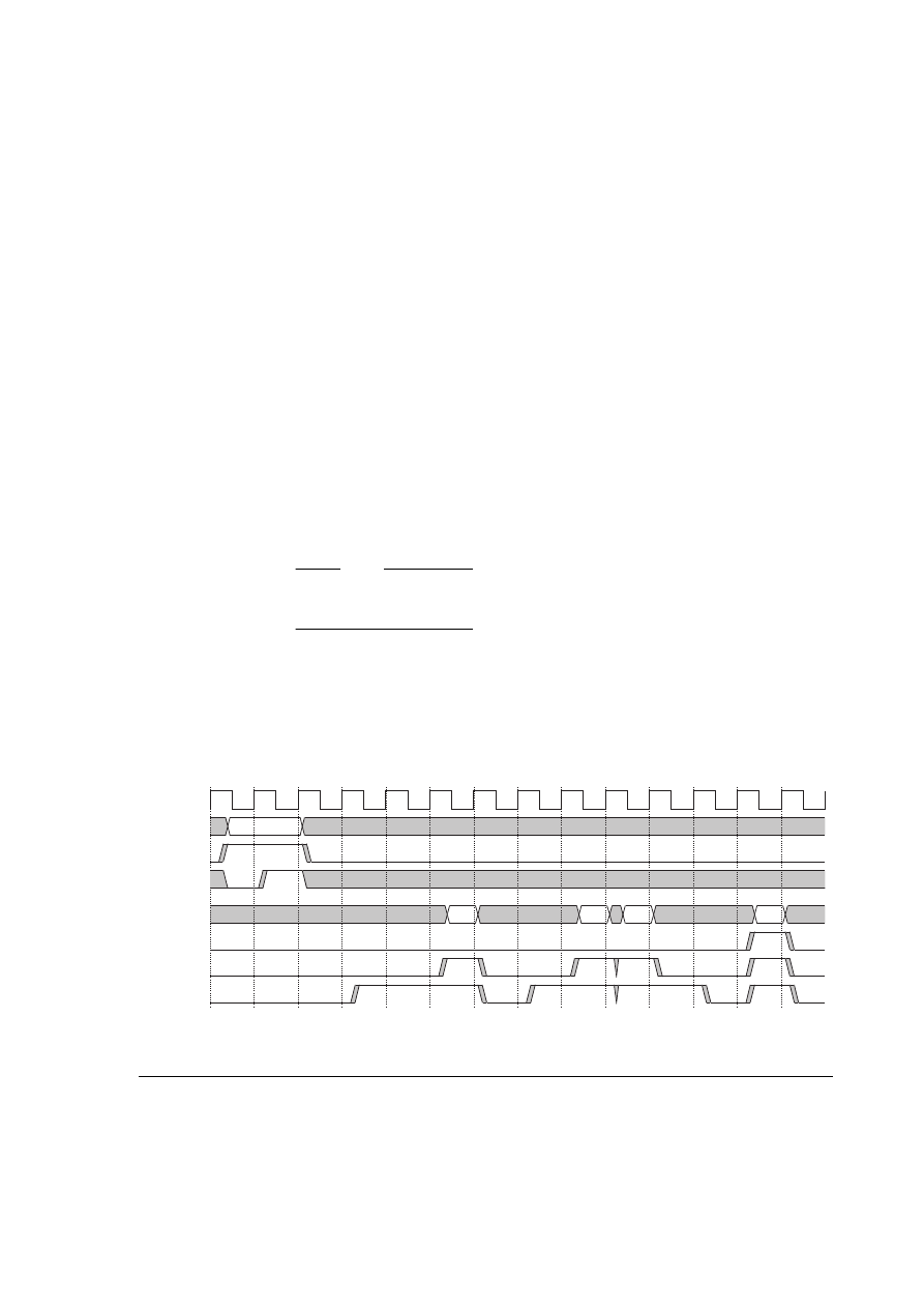
Figure 1-4 shows a read burst of four transfers. In this example, the master drives the
address, and the slave accepts it one cycle later.
Note
The master also drives a set of control signals showing the length and type of the burst,
but these signals are omitted from the figure for clarity.
After the address appears on the address bus, the data transfer occurs on the read data
channel. The slave keeps the
VALID
signal LOW until the read data is available. For
the final data transfer of the burst, the slave asserts the
RLAST
signal to show that the
last data item is being transferred.
Figure 1-4 Read burst
ARADDR
A
T12
T0
T1
T2
T3
T4
T5
T6
T7
T8
T9
T10
T11
T13
ARVALID
ARREADY
D(A0)
D(A1)
D(A2)
D(A3)
RVALID
RDATA
RLAST
RREADY
ACLK