Материал: AMBA_v30_AXI_v10

Signal Descriptions
2-6
Copyright © 2003, 2004 ARM Limited. All rights reserved.
ARM IHI 0022B
2.5
Read address channel signals
Table 2-2 on page 2-3 lists the AXI read address channel signals.
Table 2-5 Read address channel signals
Signal
Source
Description
ARID[3:0]
Master
Read address ID. This signal is the identification tag for the read address group of
signals.
ARADDR[31:0]
Master
Read address. The read address bus gives the initial address of a read burst transaction.
Only the start address of the burst is provided and the control signals that are issued
alongside the address detail how the address is calculated for the remaining transfers in
the burst.
ARLEN[3:0]
Master
Burst length. The burst length gives the exact number of transfers in a burst. This
information determines the number of data transfers associated with the address. See
Table 4-1 on page 4-3.
ARSIZE[2:0]
Master
Burst size. This signal indicates the size of each transfer in the burst. See Table 4-2 on
page 4-4.
ARBURST[1:0]
Master
Burst type. The burst type, coupled with the size information, details how the address for
each transfer within the burst is calculated. See Table 4-3 on page 4-5.
ARLOCK[1:0]
Master
Lock type. This signal provides additional information about the atomic characteristics
of the transfer. See Table 6-1 on page 6-2.
ARCACHE[3:0]
Master
Cache type. This signal provides additional information about the cacheable
characteristics of the transfer. See Table 5-1 on page 5-3.
ARPROT[2:0]
Master
Protection type. This signal provides protection unit information for the transaction. See
ARVALID
Master
Read address valid. This signal indicates, when HIGH, that the read address and control
information is valid and will remain stable until the address acknowledge signal,
ARREADY
, is high.
1 = address and control information valid
0 = address and control information not valid.
ARREADY
Slave
Read address ready. This signal indicates that the slave is ready to accept an address and
associated control signals:
1 = slave ready
0 = slave not ready.

Signal Descriptions
ARM IHI 0022B
Copyright © 2003, 2004 ARM Limited. All rights reserved.
2-7
2.6
Read data channel signals
Table 2-6 lists the AXI read data channel signals.
Table 2-6 Read data channel signals
Signal
Source
Description
RID[3:0]
Slave
Read ID tag. This signal is the ID tag of the read data group of signals. The
RID
value is
generated by the slave and must match the
ARID
value of the read transaction to which it
is responding.
RDATA[31:0]
Slave
Read data. The read data bus can be 8, 16, 32, 64, 128, 256, 512, or 1024 bits wide.
RRESP[1:0]
Slave
Read response. This signal indicates the status of the read transfer. The allowable responses
are OKAY, EXOKAY, SLVERR, and DECERR.
RLAST
Slave
Read last. This signal indicates the last transfer in a read burst.
RVALID
Slave
Read valid. This signal indicates that the required read data is available and the read
transfer can complete:
1 = read data available
0 = read data not available.
RREADY
Master
Read ready. This signal indicates that the master can accept the read data and response
information:
1= master ready
0 = master not ready.

Signal Descriptions
2-8
Copyright © 2003, 2004 ARM Limited. All rights reserved.
ARM IHI 0022B
2.7
Low-power interface signals
Table 2-7 lists the signals of the optional low-power interface.
Table 2-7 Low-power interface signals
Signal
Source
Description
CSYSREQ
Clock
controller
System low-power request. This signal is a request from the system clock controller for the
peripheral to enter a low-power state.
CSYSACK
Peripheral
device
Low-power request acknowledgement. This signal is the acknowledgement from a peripheral
of a system low-power request.
CACTIVE
Peripheral
device
Clock active. This signal indicates that the peripheral requires its clock signal:
1 = peripheral clock required
0 = peripheral clock not required.

ARM IHI 0022B
Copyright © 2003, 2004 ARM Limited. All rights reserved.
3-1
Chapter 3
Channel Handshake
This chapter describes the master/slave handshake process and outlines the
relationships and default values of the
READY
and
VALID
handshake signals. It
contains the following sections:
•
•
Relationships between the channels
•
Channel Handshake
3-2
Copyright © 2003, 2004 ARM Limited. All rights reserved.
ARM IHI 0022B
3.1
Handshake process
All five channels use the same
VALID
/
READY
handshake to transfer data and control
information. This two-way flow control mechanism enables both the master and slave
to control the rate at which the data and control information moves. The source
generates the
VALID
signal to indicate when the data or control information is
available. The destination generates the
READY
signal to indicate that it accepts the
data or control information. Transfer occurs only when both the
VALID
and
READY
signals are HIGH.
There must be no combinatorial paths between input and output signals on both master
and slave interfaces.
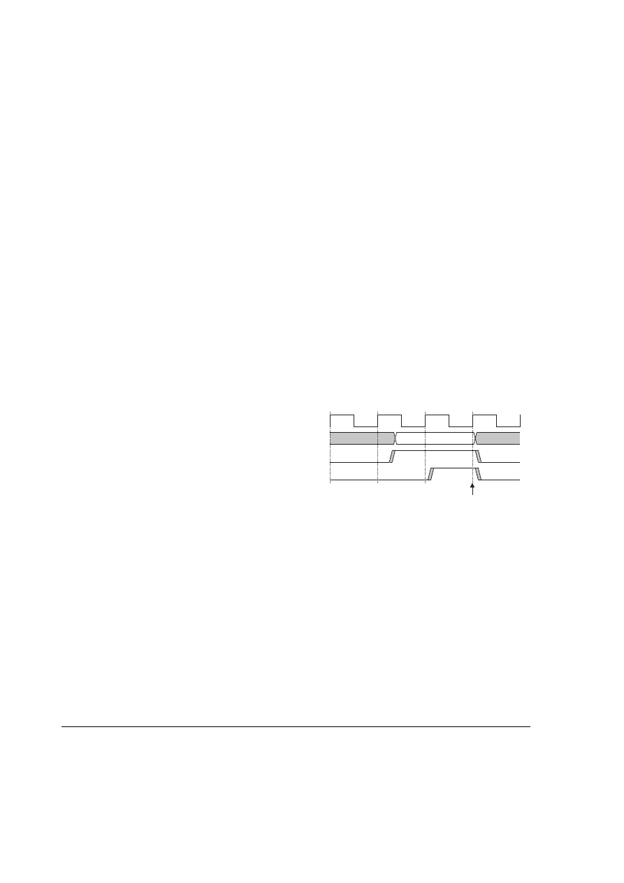
Figure 3-1 to Figure 3-3 on page 3-3 show examples of the handshake sequence. In
Figure 3-1, the source presents the data or control information and drives the
VALID
signal HIGH. The data or control information from the source remains stable until the
destination drives the
READY
signal HIGH, indicating that it accepts the data or
control information. The arrow shows when the transfer occurs.
Figure 3-1 VALID before READY handshake
In Figure 3-2 on page 3-3, the destination drives
READY
HIGH before the data or
control information is valid. This indicates that the destination can accept the data or
control information in a single cycle as soon as it becomes valid. The arrow shows when
the transfer occurs.
READY
VALID
INFORMATION
ACLK